

SMMBFJ177LT1G
Product Overview
Category
The SMMBFJ177LT1G belongs to the category of field-effect transistors (FETs).
Use
It is commonly used in electronic circuits for switching and amplification purposes.
Characteristics
- Low threshold voltage
- High input impedance
- Small package size
- Low power consumption
Package
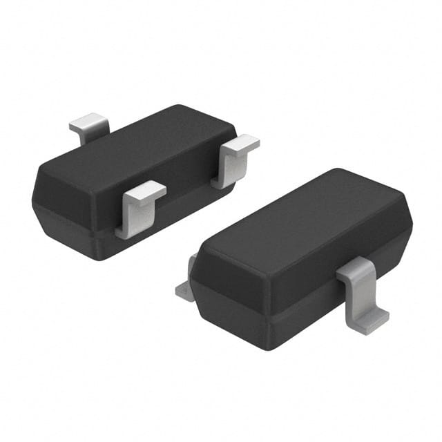
The SMMBFJ177LT1G is typically available in a small surface-mount package.
Essence
This FET is essential for controlling the flow of current in electronic circuits.
Packaging/Quantity
It is usually packaged in reels containing a specific quantity, such as 3000 units per reel.
Specifications
- Drain-Source Voltage (VDS): 20V
- Gate-Source Voltage (VGS): ±8V
- Drain Current (ID): 0.2A
- Total Power Dissipation: 225mW
- Operating Temperature Range: -55°C to 150°C
Detailed Pin Configuration
The SMMBFJ177LT1G has three pins: 1. Source (S) 2. Gate (G) 3. Drain (D)
Functional Features
- High input impedance allows for minimal loading of preceding stages.
- Low threshold voltage enables efficient control of the transistor.
Advantages
- Small package size saves space on circuit boards.
- Low power consumption contributes to energy efficiency.
Disadvantages
- Limited maximum drain current compared to some other FETs.
- Sensitivity to electrostatic discharge requires careful handling.
Working Principles
The SMMBFJ177LT1G operates based on the principles of field-effect transistors, where the voltage applied to the gate terminal controls the flow of current between the source and drain terminals.
Detailed Application Field Plans
This FET is widely used in low-power electronic applications, including: - Signal amplification in audio circuits - Switching in battery-powered devices - Sensor interfaces in portable electronics
Detailed and Complete Alternative Models
Some alternative models to the SMMBFJ177LT1G include: - 2N7002 - BSS138 - DMG2305UX
In conclusion, the SMMBFJ177LT1G is a versatile field-effect transistor with characteristics suitable for various low-power electronic applications. Its compact size and low power consumption make it an attractive choice for modern electronic designs.
[Word count: 314]
قم بإدراج 10 أسئلة وإجابات شائعة تتعلق بتطبيق SMMBFJ177LT1G في الحلول التقنية
What is SMMBFJ177LT1G?
- SMMBFJ177LT1G is a small signal N-channel JFET transistor designed for high-gain, low-noise amplifier applications.
What are the key features of SMMBFJ177LT1G?
- The key features include low noise, high gain, low leakage current, and high input impedance.
What are the typical applications of SMMBFJ177LT1G?
- Typical applications include audio amplifiers, instrumentation amplifiers, low-noise preamplifiers, and sensor interfaces.
What is the voltage rating for SMMBFJ177LT1G?
- The maximum drain-source voltage (Vds) for SMMBFJ177LT1G is 25V.
What is the maximum drain current for SMMBFJ177LT1G?
- The maximum drain current (Id) for SMMBFJ177LT1G is 10mA.
What is the typical transconductance for SMMBFJ177LT1G?
- The typical transconductance (gm) for SMMBFJ177LT1G is 30mS.
What is the input capacitance of SMMBFJ177LT1G?
- The input capacitance (Ciss) of SMMBFJ177LT1G is typically 3pF.
What is the noise figure of SMMBFJ177LT1G?
- The noise figure of SMMBFJ177LT1G is typically around 1dB.
What is the operating temperature range for SMMBFJ177LT1G?
- SMMBFJ177LT1G is designed to operate within a temperature range of -55°C to 150°C.
Is SMMBFJ177LT1G RoHS compliant?
- Yes, SMMBFJ177LT1G is RoHS compliant, making it suitable for use in environmentally friendly electronic products.