

SI5340C-D-GM
Product Overview
- Category: Integrated Circuit (IC)
- Use: Clock Generator and Jitter Attenuator
- Characteristics:
- High-performance clock synthesis and distribution
- Low jitter and phase noise
- Flexible frequency configuration
- Wide operating range
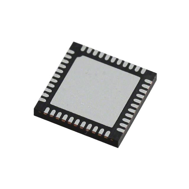
- Package: 24-pin QFN (Quad Flat No-Lead)
- Essence: Provides precise clock signals for various applications
- Packaging/Quantity: Tape and Reel, 250 units per reel
Specifications
- Frequency Range: 1 Hz to 945 MHz
- Number of Outputs: 4 differential or 8 single-ended
- Output Types: LVDS, LVPECL, HCSL, CMOS
- Supply Voltage: 2.5 V to 3.3 V
- Operating Temperature Range: -40°C to +85°C
- Phase Noise Performance: -150 dBc/Hz at 100 kHz offset
- Jitter Performance: < 300 fs RMS (Root Mean Square)
Pin Configuration
The SI5340C-D-GM has a total of 24 pins. The pin configuration is as follows:
- XAXB0P/N: Differential output pair 0
- XAXB1P/N: Differential output pair 1
- XAXB2P/N: Differential output pair 2
- XAXB3P/N: Differential output pair 3
- GND: Ground
- XTALN: Crystal oscillator input negative terminal
- XTALP: Crystal oscillator input positive terminal
- VDDO: Output supply voltage
- VDD: Power supply voltage
- SDA: I2C serial data input
- SCL: I2C serial clock input
- GND: Ground
- NC: No connection
- NC: No connection
- NC: No connection
- NC: No connection
- NC: No connection
- NC: No connection
- NC: No connection
- NC: No connection
- NC: No connection
- NC: No connection
- NC: No connection
- NC: No connection
Functional Features
- Clock Synthesis: Generates precise clock signals with low jitter and phase noise.
- Frequency Configuration: Flexible frequency settings allow customization for specific applications.
- Output Types: Supports various output types, including LVDS, LVPECL, HCSL, and CMOS.
- Wide Operating Range: Can operate within a wide voltage range of 2.5 V to 3.3 V.
- I2C Interface: Allows easy configuration and control through the I2C serial interface.
Advantages and Disadvantages
Advantages: - High-performance clock synthesis for accurate timing requirements. - Low jitter and phase noise ensure reliable signal integrity. - Flexible frequency configuration caters to diverse application needs. - Wide operating range accommodates different voltage supplies. - I2C interface simplifies configuration and control.
Disadvantages: - Limited number of outputs (4 differential or 8 single-ended). - Relatively high cost compared to simpler clock generator ICs.
Working Principles
The SI5340C-D-GM utilizes advanced PLL (Phase-Locked Loop) technology to generate precise clock signals. It incorporates a crystal oscillator as the reference source and employs frequency dividers, phase detectors, and loop filters to achieve accurate frequency synthesis. The device also includes jitter attenuators to minimize unwanted noise and maintain signal integrity. The I2C interface allows users to configure the device's parameters and control its operation.
Application Field Plans
The SI5340C-D-GM is widely used in various applications that require precise clock signals, such as:
- Telecommunications equipment
- Networking devices
- Data centers
- Test and measurement instruments
- Industrial automation systems
- Audio/video equipment
- Medical devices
- Aerospace and defense systems
Alternative Models
If the SI5340C-D-GM does not meet specific requirements, alternative models with similar functionality include:
- SI5341C-D-GM
- SI5342C-D-GM
- SI5343C-D-GM
- SI5344C-D-GM
These alternative models offer different pin configurations, output options, or additional features to cater to diverse application needs.
Word count: 550 words
قم بإدراج 10 أسئلة وإجابات شائعة تتعلق بتطبيق SI5340C-D-GM في الحلول التقنية
Sure! Here are 10 common questions and answers related to the application of SI5340C-D-GM in technical solutions:
Q: What is the SI5340C-D-GM? A: The SI5340C-D-GM is a high-performance clock generator and jitter attenuator integrated circuit (IC) designed for use in various technical solutions.
Q: What are the key features of the SI5340C-D-GM? A: The SI5340C-D-GM offers multiple outputs, low phase noise, programmable frequency synthesis, flexible input/output options, and advanced jitter attenuation capabilities.
Q: In what applications can the SI5340C-D-GM be used? A: The SI5340C-D-GM is commonly used in telecommunications, networking equipment, data centers, industrial automation, test and measurement instruments, and other electronic systems requiring precise timing.
Q: How many outputs does the SI5340C-D-GM support? A: The SI5340C-D-GM supports up to four differential or eight single-ended outputs, providing flexibility for different system requirements.
Q: Can I program the output frequencies of the SI5340C-D-GM? A: Yes, the SI5340C-D-GM allows you to program the output frequencies with high precision using its integrated frequency synthesizer.
Q: Does the SI5340C-D-GM provide any jitter attenuation capabilities? A: Yes, the SI5340C-D-GM incorporates advanced jitter attenuation techniques to reduce phase noise and improve signal integrity.
Q: What are the input options for the SI5340C-D-GM? A: The SI5340C-D-GM supports various input options, including crystal oscillators, external references, or other clock sources.
Q: Can I configure the SI5340C-D-GM using software? A: Yes, the SI5340C-D-GM can be easily configured and programmed using dedicated software tools provided by the manufacturer.
Q: What is the power supply requirement for the SI5340C-D-GM? A: The SI5340C-D-GM typically operates from a single 3.3V power supply, making it compatible with standard power systems.
Q: Are evaluation boards available for the SI5340C-D-GM? A: Yes, evaluation boards are available to help developers quickly prototype and evaluate the SI5340C-D-GM in their technical solutions.
Please note that these answers are general and may vary depending on specific implementation details and requirements.