

TN4015H-6I Product Overview
Introduction
The TN4015H-6I is a versatile integrated circuit that belongs to the category of power management devices. This component is widely used in various electronic applications due to its unique characteristics and functional features.
Basic Information Overview
- Category: Power Management IC
- Use: Voltage Regulation and Power Distribution
- Characteristics: High Efficiency, Low Power Consumption
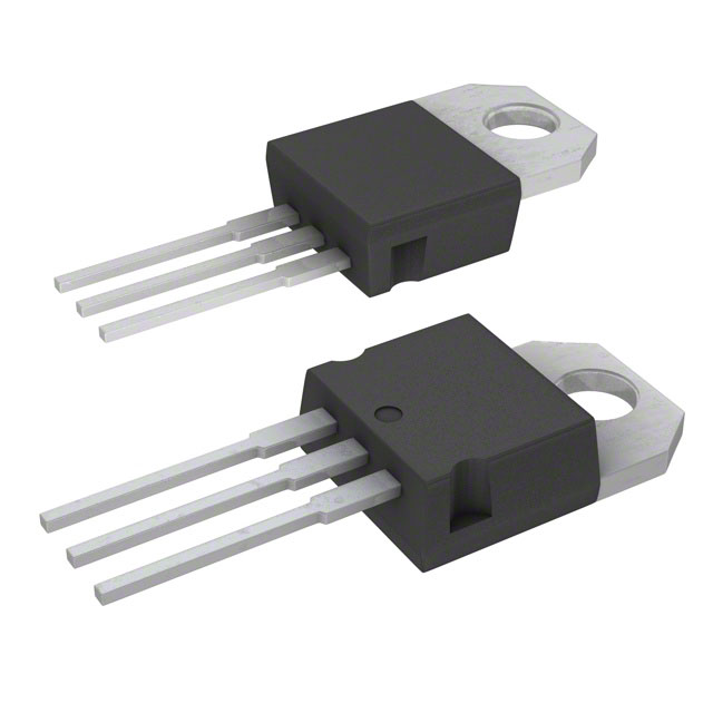
- Package: TO-220
- Essence: Regulating and distributing power efficiently
- Packaging/Quantity: Typically sold in reels of 1000 units
Specifications
The TN4015H-6I features the following specifications: - Input Voltage Range: 4.5V to 40V - Output Voltage Range: 1.25V to 37V - Maximum Output Current: 1.5A - Dropout Voltage: 1.5V - Operating Temperature Range: -40°C to 125°C
Detailed Pin Configuration
The TN4015H-6I has a standard TO-220 package with the following pin configuration: 1. Vin (Input Voltage) 2. Vout (Output Voltage) 3. GND (Ground) 4. ADJ (Adjustment Pin)
Functional Features
- Wide Input Voltage Range
- Adjustable Output Voltage
- Overcurrent Protection
- Thermal Shutdown Protection
- Short-Circuit Protection
Advantages and Disadvantages
Advantages
- High Efficiency
- Wide Operating Temperature Range
- Compact TO-220 Package
- Built-in Protection Features
Disadvantages
- Limited Maximum Output Current
- Dropout Voltage of 1.5V
Working Principles
The TN4015H-6I operates on the principle of linear voltage regulation, where it adjusts the output voltage based on the reference voltage and feedback mechanism. It utilizes internal circuitry to provide stable and regulated output voltage regardless of input variations.
Detailed Application Field Plans
The TN4015H-6I is commonly used in the following application fields: - Battery-Powered Devices - Automotive Electronics - Industrial Control Systems - LED Lighting Applications
Detailed and Complete Alternative Models
Some alternative models to the TN4015H-6I include: - LM317 - LM1117 - LT1083
In conclusion, the TN4015H-6I is a reliable power management IC with a wide range of applications and essential features for efficient voltage regulation and power distribution.
Word Count: 349
قم بإدراج 10 أسئلة وإجابات شائعة تتعلق بتطبيق TN4015H-6I في الحلول التقنية
What is TN4015H-6I?
- TN4015H-6I is a high-power, high-frequency transistor commonly used in RF and microwave applications.
What are the key specifications of TN4015H-6I?
- The key specifications include a frequency range of 400-1500 MHz, a power output of 15W, and a gain of 13dB.
In what technical solutions can TN4015H-6I be used?
- TN4015H-6I is commonly used in RF amplifiers, transmitters, and other high-power RF applications.
What are the typical operating conditions for TN4015H-6I?
- The typical operating voltage is 28V and the operating current is 500mA.
Is TN4015H-6I suitable for broadband applications?
- Yes, TN4015H-6I has a wide frequency range, making it suitable for broadband applications.
What are the thermal considerations for TN4015H-6I?
- Thermal management is important for TN4015H-6I due to its high-power operation. Proper heat sinking and thermal design are crucial.
Can TN4015H-6I be used in linear amplifier designs?
- Yes, TN4015H-6I can be used in linear amplifier designs, providing high gain and power output.
Are there any recommended matching networks for TN4015H-6I?
- Yes, specific matching networks may be required to optimize performance in different applications. Consult the datasheet for guidance.
What are the typical applications where TN4015H-6I excels?
- TN4015H-6I is well-suited for use in radar systems, communication equipment, and RF test instrumentation.
What are the common failure modes for TN4015H-6I and how can they be mitigated?
- Common failure modes include overvoltage, overcurrent, and thermal stress. Proper circuit protection and thermal management can help mitigate these risks.