

BZT55C75 L0G
Introduction
The BZT55C75 L0G is a semiconductor product belonging to the category of Zener diodes. This entry provides an overview of its basic information, specifications, pin configuration, functional features, advantages and disadvantages, working principles, application field plans, and alternative models.
Basic Information Overview
- Category: Zener Diode
- Use: Voltage regulation and protection in electronic circuits
- Characteristics: Precise voltage regulation, low impedance, and high reliability
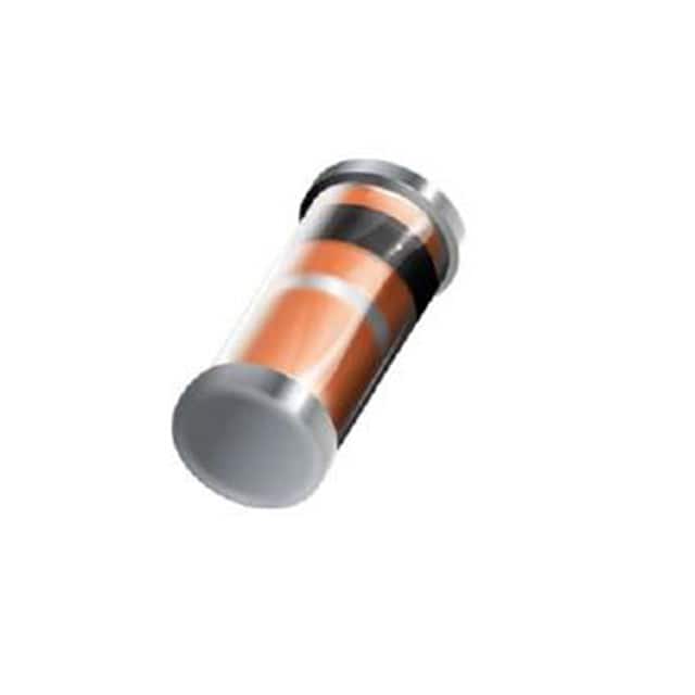
- Package: SOD-80 (MiniMELF)
- Essence: Semiconductor material with controlled reverse breakdown voltage
- Packaging/Quantity: Available in tape and reel packaging, quantity varies by supplier
Specifications
- Voltage: 75V
- Power Dissipation: 500mW
- Operating Temperature Range: -65°C to +175°C
- Zener Test Current: 20mA
Detailed Pin Configuration
The BZT55C75 L0G Zener diode has two pins, typically labeled as Anode (A) and Cathode (K).
Functional Features
- Precise Voltage Regulation: Maintains a constant voltage across its terminals, useful for stabilizing power supplies.
- Overvoltage Protection: Safeguards sensitive components in electronic circuits by limiting the voltage across them.
- Low Impedance: Allows for efficient current flow while regulating voltage.
Advantages and Disadvantages
Advantages
- Reliable voltage regulation
- Compact package size
- Low impedance for efficient operation
Disadvantages
- Limited power dissipation capability
- Susceptible to damage from excessive current or voltage spikes
Working Principles
The BZT55C75 L0G operates based on the principle of the Zener effect, where it maintains a nearly constant voltage across its terminals when reverse-biased at or above its breakdown voltage.
Detailed Application Field Plans
The BZT55C75 L0G finds applications in various electronic circuits, including: - Voltage regulators - Overvoltage protection circuits - Signal clamping circuits - Voltage reference circuits
Detailed and Complete Alternative Models
Some alternative models to the BZT55C75 L0G include: - BZX84C75 - 1N4729A - MMBZ5225B - 1SMA4753A
In conclusion, the BZT55C75 L0G Zener diode offers precise voltage regulation and overvoltage protection in a compact package, making it suitable for a wide range of electronic applications.
[Word Count: 342]
قم بإدراج 10 أسئلة وإجابات شائعة تتعلق بتطبيق BZT55C75 L0G في الحلول التقنية
What is the maximum power dissipation of BZT55C75 L0G?
- The maximum power dissipation of BZT55C75 L0G is 500mW.
What is the forward voltage drop of BZT55C75 L0G?
- The forward voltage drop of BZT55C75 L0G is typically 0.9V at a forward current of 5mA.
What is the reverse breakdown voltage of BZT55C75 L0G?
- The reverse breakdown voltage of BZT55C75 L0G is 75V.
What is the maximum continuous forward current of BZT55C75 L0G?
- The maximum continuous forward current of BZT55C75 L0G is 200mA.
What is the operating temperature range of BZT55C75 L0G?
- The operating temperature range of BZT55C75 L0G is -65°C to +150°C.
Is BZT55C75 L0G RoHS compliant?
- Yes, BZT55C75 L0G is RoHS compliant.
Can BZT55C75 L0G be used for voltage regulation in low-power applications?
- Yes, BZT55C75 L0G can be used for voltage regulation in low-power applications due to its zener diode characteristics.
What are the typical applications of BZT55C75 L0G?
- Typical applications of BZT55C75 L0G include voltage stabilization, voltage reference, and overvoltage protection in various electronic circuits.
Does BZT55C75 L0G require a heatsink for operation?
- BZT55C75 L0G does not typically require a heatsink for normal operation due to its low power dissipation.
What are the packaging options available for BZT55C75 L0G?
- BZT55C75 L0G is available in various packaging options including SOD-123, SOD-323, and DO-35 packages.