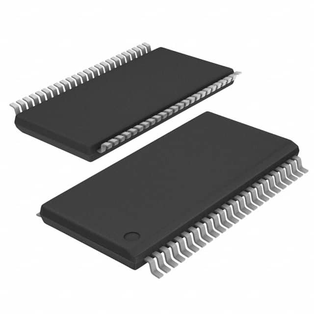
74AVC16244DGVRG4
Basic Information Overview
- Category: Integrated Circuit (IC)
- Use: Buffer/Driver
- Characteristics: High-speed, low-voltage, non-inverting
- Package: VSSOP (Very Small Outline Package)
- Essence: Provides voltage level shifting and signal buffering capabilities
- Packaging/Quantity: Tape and Reel, 2500 units per reel
Specifications
- Number of Channels: 16
- Logic Family: AVC
- Logic Type: CMOS
- Supply Voltage Range: 1.2V to 3.6V
- Input Voltage Range: 0V to VCC
- Output Voltage Range: 0V to VCC
- Maximum Operating Frequency: 400MHz
- Output Drive Capability: ±24mA
- Propagation Delay Time: 1.5ns (typical)
- Operating Temperature Range: -40°C to +85°C
Detailed Pin Configuration
The 74AVC16244DGVRG4 IC has a total of 48 pins, arranged in a dual-gate configuration. The pinout is as follows:
- Pin 1: GND (Ground)
- Pin 2: A1 (Input/Output)
- Pin 3: Y1 (Output)
- Pin 4: A2 (Input/Output)
- Pin 5: Y2 (Output)
- ...
- Pin 46: A15 (Input/Output)
- Pin 47: Y15 (Output)
- Pin 48: VCC (Supply Voltage)
Functional Features
- Non-inverting buffer/driver with 3-state outputs
- Supports bidirectional data flow
- Wide supply voltage range allows compatibility with various systems
- High-speed operation enables efficient data transfer
- Low power consumption for energy-efficient applications
- ESD protection on all inputs and outputs for enhanced reliability
Advantages and Disadvantages
Advantages: - High-speed operation enables efficient data transfer - Wide supply voltage range allows compatibility with various systems - ESD protection enhances reliability
Disadvantages: - Limited number of channels (16) - Propagation delay time may affect timing-sensitive applications
Working Principles
The 74AVC16244DGVRG4 is a non-inverting buffer/driver IC that provides voltage level shifting and signal buffering capabilities. It operates by receiving input signals and amplifying them to drive output signals with higher current capability. The 3-state outputs allow bidirectional data flow, making it suitable for bus-oriented applications.
Detailed Application Field Plans
The 74AVC16244DGVRG4 is commonly used in various electronic systems where voltage level shifting and signal buffering are required. Some specific application fields include:
- Communication Systems: Used for level translation between different logic families in communication interfaces such as UART, SPI, and I2C.
- Industrial Automation: Enables signal buffering and voltage level shifting in PLCs (Programmable Logic Controllers) and industrial control systems.
- Automotive Electronics: Facilitates data transfer between different voltage domains in automotive applications like infotainment systems and body control modules.
- Consumer Electronics: Provides signal buffering and level shifting in devices such as smartphones, tablets, and gaming consoles.
Detailed and Complete Alternative Models
- SN74LVC244A: Octal buffer/driver with 3-state outputs, compatible with 3.3V and 5V systems.
- MC74LVX4245: Octal dual-supply translating transceiver, supports voltage level shifting between different power supply domains.
- CD74HCT541: Octal buffer/driver with 3-state outputs, operates at high-speed and compatible with TTL logic levels.
(Note: The above alternative models are provided for reference and may have different specifications and pin configurations. It is recommended to refer to the respective datasheets for detailed information.)
Word count: 523 words
قم بإدراج 10 أسئلة وإجابات شائعة تتعلق بتطبيق 74AVC16244DGVRG4 في الحلول التقنية
Sure! Here are 10 common questions and answers related to the application of 74AVC16244DGVRG4 in technical solutions:
Q: What is the 74AVC16244DGVRG4? A: The 74AVC16244DGVRG4 is a 16-bit buffer/driver with 3-state outputs, designed for high-speed digital applications.
Q: What is the maximum operating voltage for the 74AVC16244DGVRG4? A: The maximum operating voltage for the 74AVC16244DGVRG4 is typically 3.6V.
Q: What is the purpose of the 3-state outputs in the 74AVC16244DGVRG4? A: The 3-state outputs allow the device to be connected to a bus or shared communication line without interfering with other devices on the same line.
Q: What is the maximum data transfer rate supported by the 74AVC16244DGVRG4? A: The 74AVC16244DGVRG4 supports high-speed data transfer rates up to several hundred megahertz.
Q: Can the 74AVC16244DGVRG4 be used in bidirectional data transmission? A: Yes, the 74AVC16244DGVRG4 can be used for bidirectional data transmission when paired with appropriate control signals.
Q: What is the typical propagation delay of the 74AVC16244DGVRG4? A: The typical propagation delay of the 74AVC16244DGVRG4 is around 2.5 nanoseconds.
Q: Is the 74AVC16244DGVRG4 compatible with different logic families? A: Yes, the 74AVC16244DGVRG4 is compatible with various logic families, including TTL, CMOS, and LVCMOS.
Q: Can the 74AVC16244DGVRG4 be used in automotive applications? A: Yes, the 74AVC16244DGVRG4 is designed to meet automotive industry standards and can be used in automotive applications.
Q: What is the power supply voltage range for the 74AVC16244DGVRG4? A: The power supply voltage range for the 74AVC16244DGVRG4 is typically between 1.2V and 3.6V.
Q: Does the 74AVC16244DGVRG4 have built-in ESD protection? A: Yes, the 74AVC16244DGVRG4 has built-in ESD protection, making it more robust against electrostatic discharge events.
Please note that these answers are general and may vary depending on the specific datasheet and manufacturer's specifications of the 74AVC16244DGVRG4.


