

74LVTH18511DGGRE4
Basic Information Overview
- Category: Integrated Circuit (IC)
- Use: Logic Level Translator
- Characteristics: High-speed, low-power, voltage-level shifting
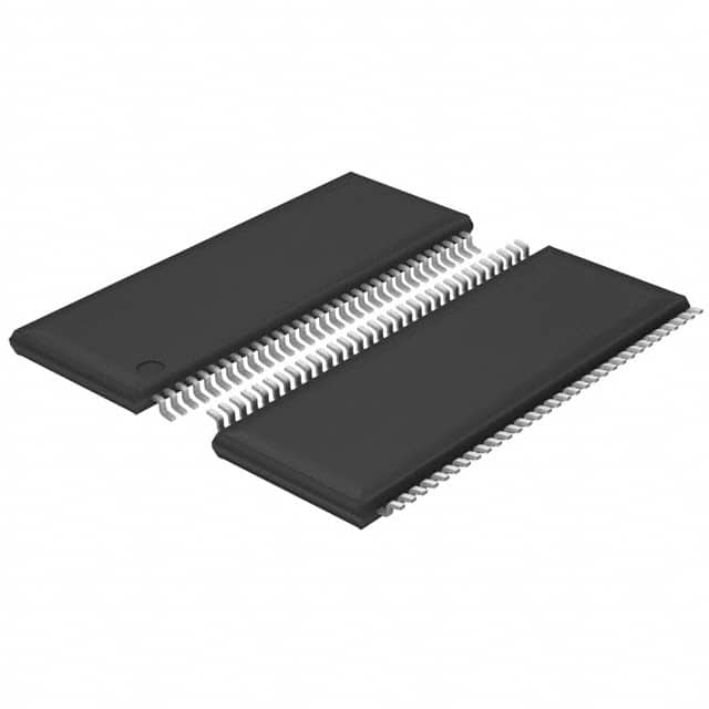
- Package: TSSOP (Thin Shrink Small Outline Package)
- Essence: Translates logic levels between different voltage domains
- Packaging/Quantity: Tape and Reel, 2500 pieces per reel
Specifications
- Supply Voltage Range: 1.65V to 5.5V
- Logic Family: LVTH
- Number of Channels: 18
- Input/Output Type: Non-Inverting
- Propagation Delay: 2.3ns (typical)
- Operating Temperature Range: -40°C to +85°C
Detailed Pin Configuration
The 74LVTH18511DGGRE4 IC has a total of 56 pins arranged in a specific configuration. The pinout diagram is as follows:
___________
      |           |
   A1 |1         56| VCC
   B1 |2         55| GND
   Y1 |3         54| A2
   Y2 |4         53| B2
   Y3 |5         52| A3
   Y4 |6         51| B3
   Y5 |7         50| A4
   Y6 |8         49| B4
   Y7 |9         48| A5
   Y8 |10        47| B5
   Y9 |11        46| A6
  Y10 |12        45| B6
  Y11 |13        44| A7
  Y12 |14        43| B7
  Y13 |15        42| A8
  Y14 |16        41| B8
  Y15 |17        40| A9
  Y16 |18        39| B9
  Y17 |19        38| A10
  Y18 |20        37| B10
   G1 |21        36| A11
   G2 |22        35| B11
   G3 |23        34| A12
   G4 |24        33| B12
   G5 |25        32| A13
   G6 |26        31| B13
   G7 |27        30| A14
   G8 |28        29| B14
      |___________|
Functional Features
- Logic Level Translation: The IC allows for bidirectional voltage-level shifting between different logic families, enabling seamless communication between devices operating at different voltage levels.
- High-Speed Operation: The 74LVTH18511DGGRE4 offers fast propagation delay, making it suitable for applications requiring quick signal transmission.
- Low Power Consumption: The IC is designed to consume minimal power, enhancing energy efficiency in electronic systems.
Advantages and Disadvantages
Advantages: - Wide supply voltage range allows compatibility with various systems. - Non-inverting input/output configuration simplifies circuit design. - High-speed operation enables efficient data transfer.
Disadvantages: - Limited number of channels may restrict its use in complex systems. - Temperature range might not be suitable for extreme environments.
Working Principles
The 74LVTH18511DGGRE4 utilizes a combination of MOSFETs and CMOS technology to achieve logic level translation. It employs a voltage divider network and level-shifting circuitry to convert signals from one voltage domain to another while maintaining signal integrity.
Detailed Application Field Plans
The 74LVTH18511DGGRE4 is commonly used in various applications, including: 1. Microcontroller interfacing: It facilitates communication between microcontrollers operating at different voltage levels. 2. Sensor networks: The IC enables level translation between sensors and microcontrollers, ensuring compatibility in mixed-voltage environments. 3. Industrial automation: It finds application in control systems where different components operate at distinct voltage levels.
Detailed and Complete Alternative Models
- SN74LVC1T45DBVR: Single-bit dual-supply bus transceiver with voltage-level translation capability.
- TXB0108PWR: Eight-channel bidirectional voltage-level translator with automatic direction sensing.
- PCA9306DCUR: Dual bidirectional I2C-bus and SMBus voltage-level translator.
These alternative models offer similar functionality and can be considered as substitutes for the 74LVTH18511DGGRE4 in specific applications.
Word count: 518 words
قم بإدراج 10 أسئلة وإجابات شائعة تتعلق بتطبيق 74LVTH18511DGGRE4 في الحلول التقنية
Sure! Here are 10 common questions and answers related to the application of 74LVTH18511DGGRE4 in technical solutions:
Q: What is the 74LVTH18511DGGRE4? A: The 74LVTH18511DGGRE4 is a 18-bit universal bus driver with 3-state outputs, designed for low-voltage (3.3V) applications.
Q: What is the purpose of the 74LVTH18511DGGRE4? A: The purpose of this IC is to provide bidirectional buffering between a high-speed bus and a low-speed or wide bus.
Q: What is the maximum operating voltage for the 74LVTH18511DGGRE4? A: The maximum operating voltage for this IC is 3.6V.
Q: Can the 74LVTH18511DGGRE4 be used in both input and output applications? A: Yes, this IC can be used as both an input buffer and an output driver.
Q: What is the maximum data rate supported by the 74LVTH18511DGGRE4? A: The maximum data rate supported by this IC is typically 400Mbps.
Q: Does the 74LVTH18511DGGRE4 have internal pull-up or pull-down resistors? A: No, this IC does not have internal pull-up or pull-down resistors.
Q: Can the 74LVTH18511DGGRE4 be used in automotive applications? A: Yes, this IC is suitable for automotive applications as it meets the AEC-Q100 standard.
Q: What is the power supply range for the 74LVTH18511DGGRE4? A: The power supply range for this IC is typically 2.7V to 3.6V.
Q: Does the 74LVTH18511DGGRE4 have overvoltage protection? A: No, this IC does not have built-in overvoltage protection. External measures should be taken to prevent overvoltage.
Q: What package options are available for the 74LVTH18511DGGRE4? A: This IC is available in a TSSOP-56 package.
Please note that these answers are general and may vary depending on the specific datasheet and manufacturer's specifications for the 74LVTH18511DGGRE4.