

ADC1001CCJ-1
Product Overview
Category
ADC1001CCJ-1 belongs to the category of Analog-to-Digital Converters (ADCs).
Use
The ADC1001CCJ-1 is used to convert analog signals into digital data. It is commonly employed in various electronic systems where precise and accurate conversion of analog signals is required.
Characteristics
- High resolution: The ADC1001CCJ-1 offers a high-resolution conversion, ensuring accurate representation of analog signals.
- Fast conversion speed: This ADC provides fast conversion times, enabling real-time data acquisition.
- Low power consumption: The ADC1001CCJ-1 is designed to consume minimal power, making it suitable for battery-powered devices.
- Wide input voltage range: It can handle a wide range of input voltages, allowing for versatile applications.
- Small package size: The compact package of the ADC1001CCJ-1 makes it suitable for space-constrained designs.
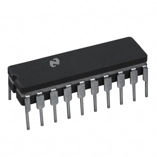
Package and Quantity
The ADC1001CCJ-1 is available in a small form factor package, typically provided in a quantity of one unit per package.
Specifications
- Resolution: 12 bits
- Conversion Speed: 1 MSPS (Mega Samples Per Second)
- Input Voltage Range: 0V to Vref
- Power Supply: 3.3V
- Operating Temperature Range: -40°C to +85°C
Pin Configuration
The detailed pin configuration of the ADC1001CCJ-1 is as follows:
Pin 1: VREF-
Pin 2: VREF+
Pin 3: GND
Pin 4: VIN
Pin 5: CLK
Pin 6: CS
Pin 7: DOUT
Pin 8: DGND
Pin 9: VDD
Functional Features
- High-resolution conversion: The ADC1001CCJ-1 provides accurate conversion of analog signals with its 12-bit resolution.
- Fast data acquisition: With a conversion speed of 1 MSPS, it enables real-time data acquisition.
- Low power consumption: The ADC1001CCJ-1 is designed to minimize power consumption, making it suitable for energy-efficient applications.
- Versatile input voltage range: It can handle a wide range of input voltages, allowing for flexibility in signal sources.
Advantages
- High accuracy: The ADC1001CCJ-1 offers precise and reliable conversion of analog signals.
- Compact size: Its small package size makes it suitable for space-constrained designs.
- Low power consumption: The ADC1001CCJ-1 helps conserve power in battery-operated devices.
Disadvantages
- Limited resolution: While the 12-bit resolution is sufficient for many applications, higher-resolution ADCs may be required for more demanding tasks.
- Single-channel: The ADC1001CCJ-1 is a single-channel ADC, limiting its capability to process multiple analog signals simultaneously.
Working Principles
The ADC1001CCJ-1 operates based on the principle of successive approximation. It samples the analog input voltage and compares it against a reference voltage. By iteratively adjusting the digital code, it converges towards an accurate representation of the analog signal.
Application Field Plans
The ADC1001CCJ-1 finds applications in various fields, including: - Industrial automation - Medical instrumentation - Data acquisition systems - Communication equipment - Automotive electronics
Alternative Models
Other alternative models that offer similar functionality to the ADC1001CCJ-1 include: - ADC1201CCJ-1: A 12-bit ADC with higher resolution. - ADC0804CCJ-1: An 8-bit ADC with lower resolution. - ADC1012CCJ-1: A 10-bit ADC with intermediate resolution.
In conclusion, the ADC1001CCJ-1 is a high-resolution analog-to-digital converter that offers fast conversion speed and low power consumption. It finds applications in various fields and is available in a compact package. While it has limitations in terms of resolution and channel count, alternative models are available to suit specific requirements.
قم بإدراج 10 أسئلة وإجابات شائعة تتعلق بتطبيق ADC1001CCJ-1 في الحلول التقنية
Sure! Here are 10 common questions and answers related to the application of ADC1001CCJ-1 in technical solutions:
Q1: What is ADC1001CCJ-1? A1: ADC1001CCJ-1 is an analog-to-digital converter (ADC) integrated circuit that converts analog signals into digital data.
Q2: What is the resolution of ADC1001CCJ-1? A2: The ADC1001CCJ-1 has a resolution of 10 bits, meaning it can represent analog signals with 2^10 (1024) discrete levels.
Q3: What is the maximum sampling rate of ADC1001CCJ-1? A3: The maximum sampling rate of ADC1001CCJ-1 is typically specified as X samples per second (SPS), where X is the value provided in the datasheet.
Q4: What is the input voltage range of ADC1001CCJ-1? A4: The input voltage range of ADC1001CCJ-1 is typically specified as Y volts, where Y is the value provided in the datasheet.
Q5: How does ADC1001CCJ-1 connect to a microcontroller or processor? A5: ADC1001CCJ-1 usually connects to a microcontroller or processor through a parallel interface, where each bit of the digital output corresponds to a specific voltage level.
Q6: Can ADC1001CCJ-1 be used for both single-ended and differential inputs? A6: Yes, ADC1001CCJ-1 supports both single-ended and differential inputs, allowing flexibility in connecting various types of analog signals.
Q7: Does ADC1001CCJ-1 require an external reference voltage? A7: Yes, ADC1001CCJ-1 typically requires an external reference voltage to accurately convert analog signals into digital data.
Q8: What is the power supply voltage range for ADC1001CCJ-1? A8: The power supply voltage range for ADC1001CCJ-1 is typically specified as Z volts, where Z is the value provided in the datasheet.
Q9: Can ADC1001CCJ-1 operate in a low-power mode? A9: Yes, ADC1001CCJ-1 often provides a low-power mode option, allowing it to consume less power when not actively converting analog signals.
Q10: Are there any application-specific considerations when using ADC1001CCJ-1? A10: Yes, some application-specific considerations include proper grounding, noise reduction techniques, and ensuring the input signal falls within the specified voltage range to achieve accurate conversions.
Please note that the specific details mentioned in the answers may vary depending on the datasheet and manufacturer's specifications of ADC1001CCJ-1.