

BUF07702PWPG4
Product Overview
- Category: Integrated Circuit (IC)
- Use: Buffer/Driver
- Characteristics:
- High-speed operation
- Low power consumption
- Wide supply voltage range
- Small package size
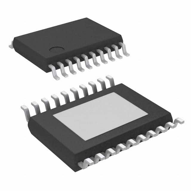
- Package: TSSOP-14
- Essence: The BUF07702PWPG4 is a high-speed buffer/driver IC designed for various applications requiring signal amplification and buffering.
- Packaging/Quantity: The BUF07702PWPG4 is available in tape and reel packaging, with 2500 units per reel.
Specifications
- Supply Voltage Range: 1.65V to 5.5V
- Operating Temperature Range: -40°C to +85°C
- Input Voltage Range: 0V to VCC
- Output Voltage Range: 0V to VCC
- Propagation Delay: 2.3ns (typical)
- Output Current: ±24mA (maximum)
Detailed Pin Configuration
The BUF07702PWPG4 has a TSSOP-14 package with the following pin configuration:
___________
      |           |
   NC |1         14| VCC
   IN |2         13| OUT
   IN |3         12| GND
   IN |4         11| NC
   IN |5         10| NC
   IN |6          9| NC
   IN |7          8| NC
      |___________|
Functional Features
- High-speed operation allows for efficient signal buffering and amplification.
- Low power consumption ensures energy efficiency in various applications.
- Wide supply voltage range enables compatibility with different power sources.
- Small package size saves board space and facilitates compact designs.
Advantages and Disadvantages
Advantages: - High-speed operation enhances signal integrity. - Low power consumption prolongs battery life in portable devices. - Wide supply voltage range increases versatility. - Small package size saves board space.
Disadvantages: - Limited output current may not be suitable for high-power applications. - Lack of ESD protection may require additional circuitry for robustness.
Working Principles
The BUF07702PWPG4 operates as a buffer/driver by receiving input signals and providing amplified output signals. It utilizes internal circuitry to ensure high-speed operation while consuming minimal power. The wide supply voltage range allows the IC to operate with different power sources, making it versatile for various applications.
Detailed Application Field Plans
The BUF07702PWPG4 is commonly used in the following application fields:
Communication Systems:
- Signal amplification in data transmission circuits
- Buffering in wireless communication modules
Audio/Video Equipment:
- Amplification of audio signals in speakers
- Buffering video signals in display devices
Industrial Automation:
- Signal conditioning in control systems
- Buffering sensor outputs for accurate measurements
Automotive Electronics:
- Amplification of signals in car audio systems
- Buffering signals in automotive displays
Detailed and Complete Alternative Models
- SN74LVC1G07DBVR: Single Buffer/Driver IC, SOT-23-5 package
- MC74VHC1GT50DTT1G: Single Buffer/Driver IC, SOT-23-6 package
- CD74HCT125M96: Quad Buffer/Driver IC, SOIC-14 package
- 74LVC244APW: Octal Buffer/Driver IC, TSSOP-20 package
These alternative models offer similar functionality and can be considered as substitutes for the BUF07702PWPG4 in various applications.
Word count: 446 words
قم بإدراج 10 أسئلة وإجابات شائعة تتعلق بتطبيق BUF07702PWPG4 في الحلول التقنية
Sure! Here are 10 common questions and answers related to the application of BUF07702PWPG4 in technical solutions:
Question: What is BUF07702PWPG4?
- Answer: BUF07702PWPG4 is a high-speed buffer and level translator integrated circuit (IC) commonly used in technical solutions.Question: What is the voltage supply range for BUF07702PWPG4?
- Answer: The voltage supply range for BUF07702PWPG4 is typically between 1.65V and 5.5V.Question: What is the maximum data rate supported by BUF07702PWPG4?
- Answer: BUF07702PWPG4 supports a maximum data rate of 100 Mbps.Question: Can BUF07702PWPG4 be used as a bidirectional level translator?
- Answer: Yes, BUF07702PWPG4 can be used as a bidirectional level translator, allowing translation between different voltage levels.Question: What is the input/output voltage range of BUF07702PWPG4?
- Answer: The input/output voltage range of BUF07702PWPG4 is typically between 0V and VCC.Question: Does BUF07702PWPG4 have built-in ESD protection?
- Answer: Yes, BUF07702PWPG4 has built-in ESD protection, providing robustness against electrostatic discharge events.Question: Can BUF07702PWPG4 be used in automotive applications?
- Answer: Yes, BUF07702PWPG4 is suitable for automotive applications, as it meets the necessary requirements for automotive environments.Question: What is the package type for BUF07702PWPG4?
- Answer: BUF07702PWPG4 is available in a small-footprint TSSOP-8 package.Question: Can BUF07702PWPG4 be used with different logic families?
- Answer: Yes, BUF07702PWPG4 is compatible with various logic families, including TTL, CMOS, and LVCMOS.Question: What are some typical applications of BUF07702PWPG4?
- Answer: BUF07702PWPG4 is commonly used in applications such as level shifting, voltage translation, clock distribution, and signal buffering in various electronic systems.
Please note that the answers provided here are general and may vary depending on specific design considerations and requirements.