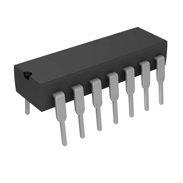
CD4041UBE
Product Overview
- Category: Integrated Circuit (IC)
- Use: Logic Gate
- Characteristics: Quad Clocked D Latch
- Package: PDIP-16 (Plastic Dual In-Line Package)
- Essence: The CD4041UBE is a quad D-type latch with clock enable. It is designed to store and transfer data in electronic systems.
- Packaging/Quantity: Available in tubes of 25 units or reels of 2,000 units.
Specifications
- Supply Voltage: 3V to 18V
- High-Level Input Voltage: 2V to VDD
- Low-Level Input Voltage: GND to 0.8V
- High-Level Output Voltage: VDD - 0.5V
- Low-Level Output Voltage: 0.5V
- Maximum Clock Frequency: 6MHz
- Operating Temperature Range: -55°C to +125°C
Detailed Pin Configuration
The CD4041UBE has a total of 16 pins, which are assigned specific functions:
- D1: Data input for latch 1
- CP1: Clock input for latch 1
- CE1: Clock enable input for latch 1
- Q1: Output for latch 1
- Q̅1: Complementary output for latch 1
- D2: Data input for latch 2
- CP2: Clock input for latch 2
- CE2: Clock enable input for latch 2
- Q2: Output for latch 2
- Q̅2: Complementary output for latch 2
- D3: Data input for latch 3
- CP3: Clock input for latch 3
- CE3: Clock enable input for latch 3
- Q3: Output for latch 3
- Q̅3: Complementary output for latch 3
- GND: Ground
Functional Features
- Quad D-type latches with individual clock enable inputs.
- Non-inverting outputs for each latch.
- High noise immunity.
- Wide operating voltage range.
- Direct interface with TTL levels.
Advantages and Disadvantages
Advantages
- Allows storage and transfer of data in electronic systems.
- Provides individual clock enable inputs for each latch.
- Offers non-inverting outputs for easy integration into various circuits.
- Suitable for applications requiring high noise immunity.
- Compatible with a wide range of operating voltages.
Disadvantages
- Limited maximum clock frequency (6MHz).
- Not suitable for high-speed applications.
- PDIP-16 package may not be ideal for space-constrained designs.
Working Principles
The CD4041UBE operates as a quad D-type latch with clock enable functionality. Each latch can store one bit of data, which is transferred to the output when the clock input is triggered. The clock enable input allows control over the transfer of data from the input to the output. The non-inverting outputs provide the stored data in its original form.
Detailed Application Field Plans
The CD4041UBE can be used in various applications, including:
- Data storage and transfer in microcontrollers and microprocessors.
- Address decoding in memory systems.
- State storage in digital communication systems.
- Control signal generation in industrial automation.
- Sequential logic circuits in digital electronics.
Detailed and Complete Alternative Models
Some alternative models that offer similar functionality to the CD4041UBE are:
- SN74HC574N: Octal D-type flip-flop with clock enable.
- CD4013BE: Dual D-type flip-flop with set and reset.
- MC14013BCL: Dual D-type flip-flop with set and reset.
These alternatives can be considered based on specific requirements and compatibility with the existing system.
Word count: 443 words
قم بإدراج 10 أسئلة وإجابات شائعة تتعلق بتطبيق CD4041UBE في الحلول التقنية
Sure! Here are 10 common questions and answers related to the application of CD4041UBE in technical solutions:
Q: What is CD4041UBE? A: CD4041UBE is a CMOS quad true/complement buffer/latch IC (Integrated Circuit) that can be used for various digital logic applications.
Q: What is the voltage supply range for CD4041UBE? A: The voltage supply range for CD4041UBE is typically between 3V and 15V.
Q: Can CD4041UBE be used as a level shifter? A: Yes, CD4041UBE can be used as a level shifter to convert signals from one voltage level to another.
Q: How many input/output pins does CD4041UBE have? A: CD4041UBE has four input pins and four output pins, making it suitable for quad logic operations.
Q: What is the maximum operating frequency of CD4041UBE? A: The maximum operating frequency of CD4041UBE is typically around 6 MHz.
Q: Can CD4041UBE be used for signal buffering? A: Yes, CD4041UBE can be used as a buffer to isolate and amplify digital signals.
Q: Is CD4041UBE compatible with TTL (Transistor-Transistor Logic) inputs? A: Yes, CD4041UBE is compatible with both TTL and CMOS logic levels.
Q: Can CD4041UBE be used for latch applications? A: Yes, CD4041UBE can be used as a latch to store and hold data until it is updated.
Q: What is the typical power consumption of CD4041UBE? A: The typical power consumption of CD4041UBE is relatively low, making it suitable for battery-powered applications.
Q: Can CD4041UBE be cascaded to increase the number of inputs/outputs? A: Yes, multiple CD4041UBE ICs can be cascaded together to increase the number of inputs and outputs in a digital circuit.
Please note that these answers are general and may vary depending on specific datasheet specifications and application requirements.


