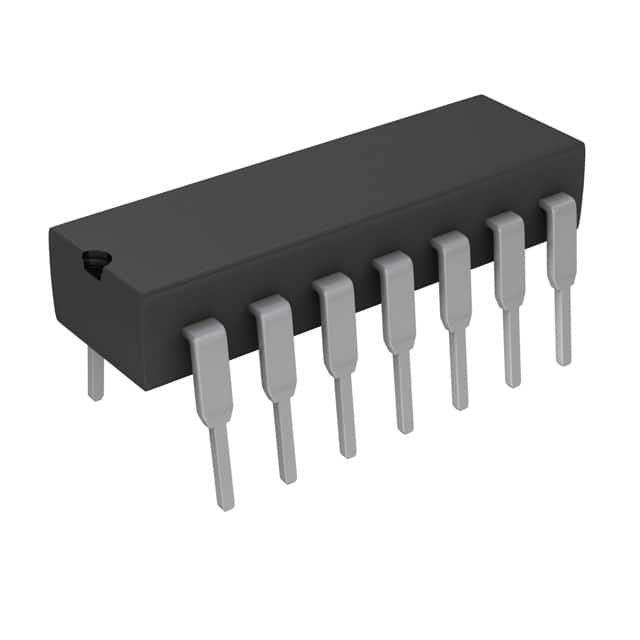
CD74HC21E
Product Overview
- Category: Integrated Circuit
- Use: Logic Gates
- Characteristics: High-Speed CMOS, Dual 4-Input AND Gate
- Package: PDIP-14
- Essence: The CD74HC21E is a dual 4-input AND gate that belongs to the high-speed CMOS logic family. It provides a fast and efficient way to perform logical AND operations on multiple inputs.
- Packaging/Quantity: The CD74HC21E is typically sold in packs of 10 or 25 units.
Specifications
- Supply Voltage: 2V to 6V
- Logic Family: HC
- Number of Inputs: 4 per gate
- Number of Gates: 2
- Propagation Delay: 9 ns (typical)
- Operating Temperature Range: -40°C to 85°C
Pin Configuration
The CD74HC21E has a 14-pin dual in-line package (PDIP-14) with the following pin configuration:
+---+--+---+
   A1 -|1  +--+ 14|- VCC
   B1 -|2       13|- C1
   A2 -|3       12|- B2
   B2 -|4  CD74HC21E 11|- A3
   Y1 -|5       10|- B3
   Y2 -|6        9|- A4
  GND -|7        8|- B4
       +----------+
Functional Features
- Dual 4-input AND gates allow for logical AND operations on four input signals simultaneously.
- High-speed CMOS technology enables fast switching times and low power consumption.
- Wide operating voltage range makes it compatible with various digital systems.
- Schmitt-trigger inputs provide hysteresis, improving noise immunity and signal integrity.
Advantages and Disadvantages
Advantages: - High-speed operation allows for efficient processing of logic operations. - Low power consumption makes it suitable for battery-powered devices. - Wide operating voltage range provides flexibility in different applications. - Schmitt-trigger inputs enhance noise immunity and signal quality.
Disadvantages: - Limited number of gates per package may require multiple ICs for complex logic circuits. - Propagation delay may introduce timing issues in certain high-frequency applications. - PDIP-14 package may not be suitable for space-constrained designs.
Working Principles
The CD74HC21E operates based on the principles of CMOS logic. It uses MOSFET transistors to implement the AND gate functionality. When all input signals are high (logic level 1), the output will be high. Otherwise, the output will be low (logic level 0). The internal circuitry ensures fast switching times and low power consumption.
Application Field Plans
The CD74HC21E can be used in various digital systems and applications, including: - Arithmetic and logical units in microprocessors and microcontrollers - Data processing and control circuits - Signal conditioning and filtering circuits - Communication systems - Industrial automation and control systems
Alternative Models
If the CD74HC21E is not available or suitable for a particular application, alternative models that offer similar functionality include: - SN74HC21N - MC74HC21AN - 74HCT21
These alternatives can be considered as drop-in replacements for the CD74HC21E, with slight variations in specifications and pin configurations.
In conclusion, the CD74HC21E is a dual 4-input AND gate integrated circuit belonging to the high-speed CMOS logic family. It offers fast switching times, low power consumption, and wide operating voltage range. Its applications range from microprocessors to communication systems. Alternative models are available for compatibility and flexibility in different designs.
قم بإدراج 10 أسئلة وإجابات شائعة تتعلق بتطبيق CD74HC21E في الحلول التقنية
Sure! Here are 10 common questions and answers related to the application of CD74HC21E in technical solutions:
Q: What is CD74HC21E? A: CD74HC21E is a dual 4-input AND gate integrated circuit (IC) that is commonly used in digital logic circuits.
Q: What is the operating voltage range for CD74HC21E? A: CD74HC21E operates within a voltage range of 2V to 6V.
Q: What is the maximum output current of CD74HC21E? A: The maximum output current of CD74HC21E is typically around 5.2mA.
Q: Can CD74HC21E be used in high-speed applications? A: Yes, CD74HC21E is designed for high-speed operation and can be used in applications with fast switching requirements.
Q: How many inputs does CD74HC21E have? A: CD74HC21E has four inputs, allowing it to perform logical AND operations on up to four input signals.
Q: What is the propagation delay of CD74HC21E? A: The typical propagation delay of CD74HC21E is around 9ns.
Q: Can CD74HC21E be used in both CMOS and TTL logic systems? A: Yes, CD74HC21E is compatible with both CMOS and TTL logic levels, making it versatile for various applications.
Q: Is CD74HC21E sensitive to noise or voltage spikes? A: CD74HC21E has built-in protection against noise and voltage spikes, ensuring reliable operation in noisy environments.
Q: Can CD74HC21E drive capacitive loads directly? A: CD74HC21E has limited output drive capability and may require additional buffering to drive capacitive loads.
Q: What is the package type for CD74HC21E? A: CD74HC21E is available in various package types, such as DIP (Dual Inline Package) and SOIC (Small Outline Integrated Circuit).
Please note that these answers are general and may vary depending on the specific datasheet and manufacturer's specifications for CD74HC21E.


