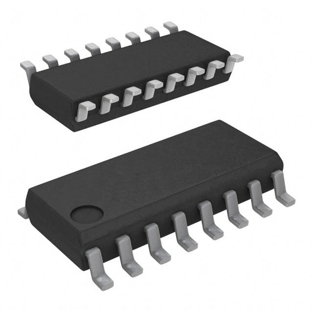
CD74HCT139M
Product Overview
Category
CD74HCT139M belongs to the category of integrated circuits (ICs).
Use
This IC is commonly used in digital electronics for decoding and demultiplexing applications.
Characteristics
- High-speed operation
- Wide operating voltage range
- Low power consumption
- Schmitt-trigger inputs for noise immunity
- Balanced propagation delays
Package
CD74HCT139M is available in a 16-pin SOIC (Small Outline Integrated Circuit) package.
Essence
The essence of CD74HCT139M lies in its ability to decode binary-coded inputs into separate outputs, making it suitable for various digital applications.
Packaging/Quantity
CD74HCT139M is typically packaged in reels or tubes, with a quantity of 2500 units per reel/tube.
Specifications
- Supply Voltage: 2V to 6V
- Input Voltage: 0V to VCC
- Output Voltage: 0V to VCC
- Operating Temperature Range: -40°C to +85°C
- Logic Family: HCT
- Number of Inputs: 2
- Number of Outputs: 4
Detailed Pin Configuration
- GND (Ground)
- A0 (Input A0)
- A1 (Input A1)
- Y0 (Output Y0)
- Y1 (Output Y1)
- Y2 (Output Y2)
- Y3 (Output Y3)
- VCC (Supply Voltage)
Functional Features
- Decodes binary-coded inputs into separate outputs
- Provides demultiplexing functionality
- High-speed operation allows for efficient data processing
- Schmitt-trigger inputs ensure noise immunity
- Balanced propagation delays enable accurate timing
Advantages
- Wide operating voltage range allows for compatibility with various systems
- Low power consumption results in energy-efficient operation
- Schmitt-trigger inputs enhance noise immunity, ensuring reliable performance
- Balanced propagation delays enable precise timing synchronization
Disadvantages
- Limited number of inputs and outputs restricts the complexity of applications
- Availability may vary depending on the supplier and market demand
Working Principles
CD74HCT139M works by receiving binary-coded inputs (A0 and A1) and decoding them into separate outputs (Y0, Y1, Y2, and Y3). The selected output line corresponds to the input combination, allowing for demultiplexing functionality. The IC operates at high speed, ensuring efficient data processing.
Detailed Application Field Plans
CD74HCT139M finds application in various digital systems, including: - Address decoding in microcontrollers and microprocessors - Data routing in multiplexers and demultiplexers - Signal selection in audio/video equipment - Control logic in communication systems
Detailed and Complete Alternative Models
Some alternative models that offer similar functionality to CD74HCT139M are: - 74HC139: This IC is compatible with a wide range of supply voltages and offers multiple package options. - CD4016: This analog switch IC provides similar demultiplexing functionality but with a higher number of inputs and outputs. - SN74LS138: This decoder/demultiplexer IC operates at higher speeds and offers additional features like active-low outputs.
(Note: The above alternative models are provided as examples and may not cover all available options.)
Word count: 446 words
قم بإدراج 10 أسئلة وإجابات شائعة تتعلق بتطبيق CD74HCT139M في الحلول التقنية
Sure! Here are 10 common questions and answers related to the application of CD74HCT139M in technical solutions:
Q: What is CD74HCT139M? A: CD74HCT139M is a dual 2-to-4 line decoder/demultiplexer integrated circuit (IC) that can be used in various digital logic applications.
Q: What is the purpose of CD74HCT139M? A: CD74HCT139M is used to decode binary information from two input lines into four output lines, making it useful for addressing, data routing, and selection purposes.
Q: What is the operating voltage range for CD74HCT139M? A: CD74HCT139M operates within a voltage range of 2V to 6V, making it compatible with both TTL and CMOS logic levels.
Q: How many inputs does CD74HCT139M have? A: CD74HCT139M has two input lines, labeled A and B, which are used to select one of the four output lines.
Q: How many output lines does CD74HCT139M have? A: CD74HCT139M has four output lines, labeled Y0, Y1, Y2, and Y3, which correspond to the possible combinations of the input lines.
Q: Can CD74HCT139M be cascaded to increase the number of output lines? A: Yes, multiple CD74HCT139M ICs can be cascaded together to increase the number of output lines by connecting the enable (E) pin of subsequent ICs to the output of the previous IC.
Q: What is the maximum frequency at which CD74HCT139M can operate? A: CD74HCT139M has a maximum operating frequency of 25 MHz, making it suitable for high-speed digital applications.
Q: Is CD74HCT139M capable of driving external loads directly? A: CD74HCT139M can drive standard TTL or CMOS logic levels but may require additional buffering if driving heavy loads or long traces.
Q: What is the power supply current requirement for CD74HCT139M? A: The typical power supply current for CD74HCT139M is around 4 mA, but it can vary depending on the specific operating conditions.
Q: Are there any special considerations when using CD74HCT139M in noisy environments? A: It is recommended to use bypass capacitors near the power supply pins of CD74HCT139M to minimize noise and ensure stable operation in noisy environments.
Please note that these answers are general and may vary based on the specific application and circuit design. Always refer to the datasheet and consult with an electronics professional for accurate information.


