

CDCE62005RGZR
Overview
Category
CDCE62005RGZR belongs to the category of integrated circuits (ICs).
Use
It is commonly used as a clock generator and frequency synthesizer in electronic devices.
Characteristics
- CDCE62005RGZR has high precision and stability in generating clock signals.
- It offers programmable output frequencies and phase-locked loop (PLL) functionality.
- The device operates at low power consumption and supports various input and output formats.
Package
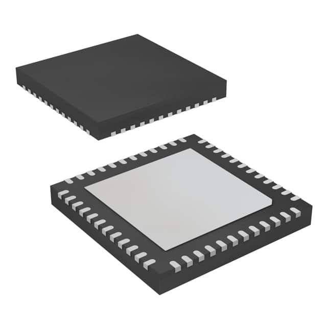
CDCE62005RGZR is available in a small form factor package, such as QFN or BGA.
Essence
The essence of CDCE62005RGZR lies in its ability to generate accurate clock signals for synchronization purposes in electronic systems.
Packaging/Quantity
The product is typically packaged in reels or trays, with a quantity of 250 or more units per package.
Specifications and Parameters
CDCE62005RGZR features the following specifications and parameters:
- Input Voltage Range: 1.8V - 3.3V
- Output Frequency Range: 1MHz - 200MHz
- Supply Voltage: 2.5V - 3.3V
- Operating Temperature Range: -40°C to +85°C
- Package Type: QFN or BGA
Pin Configuration
The pin configuration of CDCE62005RGZR is as follows:
- VDD
- GND
- XIN
- XOUT
- CLKIN
- CLKOUT0
- CLKOUT1
- CLKOUT2
- CLKOUT3
- SDA
- SCL
- OE
Functional Characteristics
CDCE62005RGZR offers the following functional characteristics:
- Clock signal generation with programmable frequencies
- Phase-locked loop (PLL) functionality for precise synchronization
- Multiple output channels for versatile system integration
- I2C interface for easy configuration and control
Advantages and Disadvantages
Advantages
- High precision and stability in clock signal generation
- Programmable output frequencies for flexibility
- Low power consumption for energy efficiency
- Compact form factor for space-constrained designs
Disadvantages
- Limited output frequency range compared to some specialized clock generators
- Requires external components for proper operation
Applicable Range of Products
CDCE62005RGZR is suitable for use in a wide range of electronic products, including:
- Communication devices
- Computer systems
- Consumer electronics
- Industrial equipment
- Automotive applications
Working Principles
The working principle of CDCE62005RGZR involves taking an input clock signal and using the internal PLL to generate multiple synchronized output clock signals. The device allows for programmable frequency division and multiplication, enabling precise timing control in various applications.
Detailed Application Field Plans
CDCE62005RGZR can be applied in the following fields:
- Wireless communication systems: Provides accurate clock signals for data transmission and reception.
- Microprocessor-based systems: Synchronizes the operation of various components for efficient processing.
- Audio/video equipment: Ensures precise timing for smooth playback and recording.
- Test and measurement instruments: Enables accurate timebase generation for precise measurements.
- Automotive electronics: Facilitates synchronization of various subsystems for reliable performance.
Detailed Alternative Models
Some alternative models to CDCE62005RGZR include:
- CDCE62002RGZR
- CDCE62003RGZR
- CDCE62004RGZR
- CDCE62006RGZR
- CDCE62007RGZR
5 Common Technical Questions and Answers
Q: What is the maximum output frequency of CDCE62005RGZR? A: The maximum output frequency is 200MHz.
Q: Can CDCE62005RGZR operate with a supply voltage of 5V? A: No, the recommended supply voltage range is 2.5V to 3.3V.
Q: Does CDCE62005RGZR support I2C communication? A: Yes, it features an I2C interface for configuration and control.
Q: What is the operating temperature range of CDCE62005RGZR? A: It can operate within the temperature range of -40°C to +85°C.
Q: Is CDCE62005RGZR RoHS compliant? A: Yes, it is compliant with the Restriction of Hazardous Substances (RoHS) directive.
This concludes the encyclopedia entry for CDCE62005RGZR.