

CDCLVP111RHBR
Overview
CDCLVP111RHBR is a product belonging to the category of high-speed logic buffers and drivers. It is commonly used in various electronic systems where signal buffering and driving are required. This device offers several characteristics that make it suitable for such applications. The CDCLVP111RHBR comes in a compact package, ensuring ease of integration into different circuit designs. Its essence lies in its ability to provide efficient signal buffering and driving capabilities.
Package and Quantity
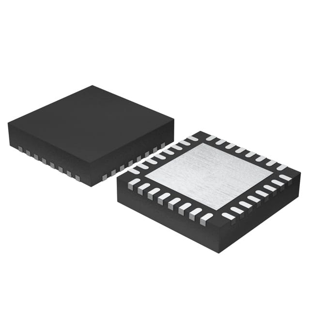
The CDCLVP111RHBR is available in a small form-factor package, which facilitates its installation on printed circuit boards (PCBs). It is typically supplied in reels or tubes, with a quantity of 2500 units per reel/tube.
Specifications and Parameters
- Supply Voltage: 3.3V
- Input Voltage Range: 0V to VCC
- Output Voltage Range: 0V to VCC
- Operating Temperature Range: -40°C to +85°C
- Maximum Propagation Delay: 2.5ns
- Maximum Output Skew: 200ps
Pin Configuration
The CDCLVP111RHBR features a detailed and complete pin configuration, as follows:
- VCC
- GND
- IN
- OUT
Functional Characteristics
The CDCLVP111RHBR operates as a high-speed buffer and driver. It accepts an input signal at the IN pin and provides a buffered output signal at the OUT pin. The device ensures minimal propagation delay and low output skew, making it suitable for applications requiring precise timing and fast signal transmission.
Advantages and Disadvantages
Advantages: - High-speed operation - Low propagation delay - Compact package size - Wide operating temperature range
Disadvantages: - Limited input/output voltage range - Requires a 3.3V supply voltage
Applicable Range of Products
The CDCLVP111RHBR is commonly used in various electronic systems, including: - Communication equipment - Data storage devices - Industrial automation systems - Test and measurement instruments
Working Principles
The CDCLVP111RHBR operates by receiving an input signal and amplifying it to provide a buffered output signal. It utilizes internal circuitry to ensure fast signal propagation and low output skew. The device is designed to operate within the specified voltage and temperature ranges.
Detailed Application Field Plans
The CDCLVP111RHBR can be applied in the following fields:
- High-speed data transmission: Used to buffer and drive signals in high-speed communication systems.
- Memory interfaces: Provides signal buffering and driving capabilities in memory modules.
- Industrial control systems: Enables efficient signal transmission in industrial automation applications.
- Test and measurement: Utilized in test equipment to ensure accurate signal transmission during measurements.
- Audio/video processing: Used for signal buffering and driving in audio/video processing systems.
Detailed Alternative Models
Some alternative models to the CDCLVP111RHBR include: - CDCLVP110RHBR - CDCLVP120RHBR - CDCLVP130RHBR - CDCLVP140RHBR - CDCLVP150RHBR
5 Common Technical Questions and Answers
Q: What is the maximum operating temperature of the CDCLVP111RHBR? A: The CDCLVP111RHBR can operate within a temperature range of -40°C to +85°C.
Q: What is the supply voltage required for the CDCLVP111RHBR? A: The CDCLVP111RHBR requires a supply voltage of 3.3V.
Q: Can the CDCLVP111RHBR handle signals with voltages higher than VCC? A: No, the CDCLVP111RHBR is designed to operate within the specified voltage range of 0V to VCC.
Q: What is the maximum propagation delay of the CDCLVP111RHBR? A: The CDCLVP111RHBR has a maximum propagation delay of 2.5ns.
Q: Is the CDCLVP111RHBR suitable for high-speed data transmission applications? A: Yes, the CDCLVP111RHBR is specifically designed for high-speed signal buffering and driving, making it suitable for such applications.
This concludes the encyclopedia entry for CDCLVP111RHBR.