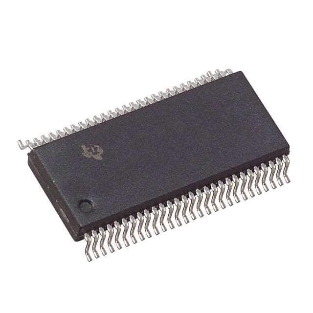
CY74FCT16543CTPVCT
Basic Information Overview
- Category: Integrated Circuit (IC)
- Use: Data storage and transfer
- Characteristics: High-speed, low-power consumption
- Package: Ceramic, 48-pin TSSOP
- Essence: 16-bit registered transceiver
- Packaging/Quantity: Tape and reel, 2500 units per reel
Specifications
- Number of Bits: 16
- Logic Family: FCT
- Supply Voltage: 4.5V to 5.5V
- Input/Output Type: CMOS/TTL compatible
- Operating Temperature Range: -40°C to +85°C
- Output Drive Capability: ±24mA
- Propagation Delay: 3.5ns (max)
- Power Dissipation: 500mW (max)
Detailed Pin Configuration
- A1: Data Input A1
- B1: Data Input B1
- G1: Output Enable Input for Port A
- CP: Clock Pulse Input
- D1: Data Input D1
- D2: Data Input D2
- GND: Ground
- Q1: Data Output Q1
- Q2: Data Output Q2
- VCC: Positive Supply Voltage
- A2: Data Input A2
- B2: Data Input B2
- G2: Output Enable Input for Port B
- OEAB: Output Enable Input for Ports A and B
- D3: Data Input D3
- D4: Data Input D4
- Q3: Data Output Q3
- Q4: Data Output Q4
- A3: Data Input A3
- B3: Data Input B3
- G3: Output Enable Input for Port C
- CPAB: Clock Pulse Input for Ports A and B
- D5: Data Input D5
- D6: Data Input D6
- Q5: Data Output Q5
- Q6: Data Output Q6
- A4: Data Input A4
- B4: Data Input B4
- G4: Output Enable Input for Port D
- OECD: Output Enable Input for Ports C and D
- D7: Data Input D7
- D8: Data Input D8
- Q7: Data Output Q7
- Q8: Data Output Q8
- A5: Data Input A5
- B5: Data Input B5
- G5: Output Enable Input for Port E
- CPAB: Clock Pulse Input for Ports C and D
- D9: Data Input D9
- D10: Data Input D10
- Q9: Data Output Q9
- Q10: Data Output Q10
- A6: Data Input A6
- B6: Data Input B6
- G6: Output Enable Input for Port F
- OEA: Output Enable Input for Ports E and F
- D11: Data Input D11
- D12: Data Input D12
Functional Features
- 16-bit registered transceiver with output enable control
- Bidirectional data flow capability
- Non-inverting outputs
- Separate clock and output enable inputs for each port
- High-speed operation with low power consumption
- TTL-compatible inputs for easy interfacing with other logic families
Advantages
- High-speed data transfer with minimal propagation delay
- Low power consumption, suitable for battery-powered devices
- Bidirectional data flow allows for versatile applications
- Wide operating temperature range enables usage in various environments
- Compatibility with different logic families simplifies integration
Disadvantages
- Limited output drive capability may restrict use in certain applications requiring higher current levels
- 16-bit width may not be sufficient for larger data transfer requirements
- Ceramic package may be more expensive compared to other packaging options
Working Principles
The CY74FCT16543CTPVCT is a 16-bit registered transceiver that allows bidirectional data transfer between two ports. The device operates based on clock pulses and output enable signals. When the clock pulse is active, data from the input pins is latched into the internal registers. The output enable control determines whether the data is transmitted to the output pins or held in the registers.
Detailed Application Field Plans
- Data communication systems
- Microprocessor interfacing
- Memory modules
- Industrial automation
- Telecommunications equipment
Detailed and Complete Alternative Models
- SN74FCT16543CTPVCT
- MC74FCT16543CTPVCT
قم بإدراج 10 أسئلة وإجابات شائعة تتعلق بتطبيق CY74FCT16543CTPVCT في الحلول التقنية
Sure! Here are 10 common questions and answers related to the application of CY74FCT16543CTPVCT in technical solutions:
Question: What is the function of CY74FCT16543CTPVCT?
Answer: CY74FCT16543CTPVCT is a 16-bit registered transceiver with 3-state outputs. It can be used for bidirectional data transfer between two buses.Question: What is the voltage range supported by CY74FCT16543CTPVCT?
Answer: CY74FCT16543CTPVCT supports a voltage range of 4.5V to 5.5V.Question: Can CY74FCT16543CTPVCT handle high-speed data transfer?
Answer: Yes, CY74FCT16543CTPVCT is designed to operate at high speeds, making it suitable for applications requiring fast data transfer.Question: How many data inputs and outputs does CY74FCT16543CTPVCT have?
Answer: CY74FCT16543CTPVCT has 16 data inputs and 16 data outputs.Question: Does CY74FCT16543CTPVCT support 3-state outputs?
Answer: Yes, CY74FCT16543CTPVCT has 3-state outputs, allowing multiple devices to share a bus without interfering with each other.Question: Can CY74FCT16543CTPVCT be cascaded to increase the number of input/output lines?
Answer: Yes, multiple CY74FCT16543CTPVCT devices can be cascaded to increase the number of input/output lines in a system.Question: What is the maximum operating frequency of CY74FCT16543CTPVCT?
Answer: The maximum operating frequency of CY74FCT16543CTPVCT is typically around 200 MHz.Question: Is CY74FCT16543CTPVCT compatible with TTL and CMOS logic levels?
Answer: Yes, CY74FCT16543CTPVCT is compatible with both TTL and CMOS logic levels, making it versatile for various applications.Question: Can CY74FCT16543CTPVCT be used in automotive applications?
Answer: Yes, CY74FCT16543CTPVCT is designed to meet the requirements of automotive applications, including temperature and voltage ranges.Question: Are there any special considerations for PCB layout when using CY74FCT16543CTPVCT?
Answer: It is recommended to follow the guidelines provided in the datasheet for proper PCB layout, including signal integrity and decoupling capacitor placement.
Please note that these answers are general and may vary depending on specific application requirements. It is always advisable to refer to the datasheet and consult with technical experts for accurate information.


