

DAC5662MPFBEP
Product Overview
- Category: Digital-to-Analog Converter (DAC)
- Use: Converts digital signals into analog signals
- Characteristics:
- High resolution and accuracy
- Low power consumption
- Wide operating temperature range
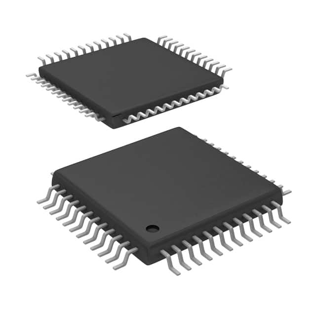
- Package: MPFBEP (MicroPad Flip Chip Bumpless EP)
- Essence: Provides high-quality analog output for various applications
- Packaging/Quantity: Available in tape and reel packaging, quantity varies based on customer requirements
Specifications
- Resolution: 16-bit
- Sampling Rate: Up to 1 MSPS (Mega Samples Per Second)
- Voltage Reference Range: 0V to VREF
- Power Supply Range: 2.7V to 5.5V
- Operating Temperature Range: -40°C to +85°C
- Interface: Serial Peripheral Interface (SPI)
Detailed Pin Configuration
The DAC5662MPFBEP has the following pin configuration:
- VDD: Power supply voltage
- GND: Ground reference
- DIN: Serial data input
- SCLK: Serial clock input
- CS: Chip select input
- LDAC: Load DAC input
- REF: Voltage reference input
- OUT: Analog output
Functional Features
- High-resolution conversion with 16-bit accuracy
- Fast sampling rate of up to 1 MSPS
- Low power consumption for energy-efficient operation
- Wide operating temperature range allows for use in various environments
- SPI interface enables easy integration with microcontrollers and other devices
Advantages and Disadvantages
Advantages: - High resolution and accuracy provide precise analog output - Low power consumption helps conserve energy - Wide operating temperature range ensures reliability in different conditions
Disadvantages: - Limited voltage reference range may restrict certain applications - Requires external components for voltage reference and power supply
Working Principles
The DAC5662MPFBEP works by converting digital input signals into corresponding analog output voltages. It utilizes a 16-bit resolution to provide high precision in the conversion process. The device receives serial data input through the DIN pin and uses the SCLK signal for synchronization. The CS pin is used to select the DAC, and the LDAC pin allows for simultaneous updating of multiple DACs. The REF pin is used to provide the voltage reference for accurate conversion. The analog output is available at the OUT pin.
Detailed Application Field Plans
The DAC5662MPFBEP can be used in various applications, including: 1. Audio Systems: Provides high-quality analog audio output for amplifiers, speakers, and headphones. 2. Instrumentation: Enables precise control of analog signals in measurement and testing equipment. 3. Industrial Automation: Used in control systems to generate analog control signals for actuators and sensors. 4. Communication Systems: Converts digital signals into analog for transmission or modulation purposes. 5. Automotive Electronics: Integrates into automotive systems for audio processing, sensor calibration, and control.
Detailed and Complete Alternative Models
- DAC5682MPFBEP: Similar to DAC5662MPFBEP but with higher resolution (18-bit).
- DAC5642MPFBEP: Similar to DAC5662MPFBEP but with lower resolution (14-bit).
- DAC5672MPFBEP: Similar to DAC5662MPFBEP but with higher sampling rate (2 MSPS).
(Note: This list is not exhaustive and other alternative models may exist.)
Word count: 346 words
قم بإدراج 10 أسئلة وإجابات شائعة تتعلق بتطبيق DAC5662MPFBEP في الحلول التقنية
Sure! Here are 10 common questions and answers related to the application of DAC5662MPFBEP in technical solutions:
Q: What is DAC5662MPFBEP? A: DAC5662MPFBEP is a digital-to-analog converter (DAC) integrated circuit that converts digital signals into analog signals.
Q: What is the operating voltage range of DAC5662MPFBEP? A: The operating voltage range of DAC5662MPFBEP is typically between 2.7V and 5.5V.
Q: What is the resolution of DAC5662MPFBEP? A: DAC5662MPFBEP has a resolution of 16 bits, which means it can represent 2^16 (65,536) different analog output levels.
Q: What is the maximum sampling rate supported by DAC5662MPFBEP? A: DAC5662MPFBEP supports a maximum sampling rate of 500 kilosamples per second (ksps).
Q: Can DAC5662MPFBEP be used in audio applications? A: Yes, DAC5662MPFBEP can be used in audio applications such as audio playback devices, audio mixers, and musical instruments.
Q: Does DAC5662MPFBEP support multiple output channels? A: No, DAC5662MPFBEP is a single-channel DAC, meaning it can generate one analog output signal at a time.
Q: What is the power consumption of DAC5662MPFBEP? A: The power consumption of DAC5662MPFBEP depends on various factors, but typically ranges from a few milliwatts to a few watts.
Q: Can DAC5662MPFBEP be controlled using a microcontroller or a digital interface? A: Yes, DAC5662MPFBEP can be controlled using standard digital interfaces such as SPI (Serial Peripheral Interface) or I2C (Inter-Integrated Circuit).
Q: What is the output voltage range of DAC5662MPFBEP? A: The output voltage range of DAC5662MPFBEP depends on the reference voltage provided to it. It can typically cover the full-scale range of the reference voltage.
Q: Are there any evaluation boards or development kits available for DAC5662MPFBEP? A: Yes, Texas Instruments provides evaluation boards and development kits for DAC5662MPFBEP, which can help in prototyping and testing applications using this DAC.
Please note that these answers are general and may vary depending on the specific implementation and datasheet of DAC5662MPFBEP.