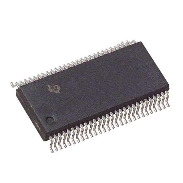
SN74ABT162501DL
Product Overview
- Category: Integrated Circuit
- Use: Data Buffer/Driver
- Characteristics: High-speed, Non-inverting, 16-bit, Tri-state
- Package: TSSOP (Thin Shrink Small Outline Package)
- Essence: Buffering and driving data signals in digital systems
- Packaging/Quantity: Tape and Reel, 2500 units per reel
Specifications
- Logic Family: ABT
- Number of Bits: 16
- Input Voltage Range: 2V to 5.5V
- Output Voltage Range: 0V to VCC
- Operating Temperature Range: -40°C to 85°C
- Propagation Delay Time: 3.8ns (typical)
- Output Drive Capability: ±24mA
- Supply Voltage: 4.5V to 5.5V
Detailed Pin Configuration
The SN74ABT162501DL has a total of 56 pins. The pin configuration is as follows:
- OE (Output Enable) 1
- Y0 (Output) 1
- GND (Ground)
- Y1 (Output) 1
- Y2 (Output) 1
- Y3 (Output) 1
- Y4 (Output) 1
- Y5 (Output) 1
- Y6 (Output) 1
- Y7 (Output) 1
- Y8 (Output) 1
- Y9 (Output) 1
- Y10 (Output) 1
- Y11 (Output) 1
- Y12 (Output) 1
- Y13 (Output) 1
- VCC (Supply Voltage)
- Y14 (Output) 1
- Y15 (Output) 1
- GND (Ground)
- A0 (Input) 1
- A1 (Input) 1
- A2 (Input) 1
- A3 (Input) 1
- A4 (Input) 1
- A5 (Input) 1
- A6 (Input) 1
- A7 (Input) 1
- A8 (Input) 1
- A9 (Input) 1
- A10 (Input) 1
- A11 (Input) 1
- A12 (Input) 1
- A13 (Input) 1
- A14 (Input) 1
- A15 (Input) 1
- VCC (Supply Voltage)
- OE (Output Enable) 2
- Y0 (Output) 2
- GND (Ground)
- Y1 (Output) 2
- Y2 (Output) 2
- Y3 (Output) 2
- Y4 (Output) 2
- Y5 (Output) 2
- Y6 (Output) 2
- Y7 (Output) 2
- Y8 (Output) 2
- Y9 (Output) 2
- Y10 (Output) 2
- Y11 (Output) 2
- Y12 (Output) 2
- Y13 (Output) 2
- VCC (Supply Voltage)
- Y14 (Output) 2
- Y15 (Output) 2
Functional Features
- Non-inverting buffer/driver
- Tri-state outputs for bus-oriented applications
- High-speed operation suitable for high-frequency systems
- Wide input voltage range allows compatibility with various logic families
- Output drive capability enables driving of capacitive loads
Advantages and Disadvantages
Advantages: - Non-inverting buffer preserves the signal integrity - Tri-state outputs allow multiple devices to share a common bus - High-speed operation enhances system performance - Wide input voltage range provides flexibility in interfacing with different logic families
Disadvantages: - Limited output drive capability may restrict usage in certain applications requiring higher current sourcing/sinking - TSSOP package may be challenging for manual soldering due to its small size
Working Principles
The SN74ABT162501DL is a 16-bit non-inverting buffer/driver designed to provide high-speed signal buffering and driving capabilities. It operates on a supply voltage range of 4.5V to 5.5V, making it compatible with various digital systems. The device features tri-state outputs, allowing multiple devices to share a common bus without interfering with each other.
When the output enable (OE)
قم بإدراج 10 أسئلة وإجابات شائعة تتعلق بتطبيق SN74ABT162501DL في الحلول التقنية
Sure! Here are 10 common questions and answers related to the application of SN74ABT162501DL:
Q: What is SN74ABT162501DL? A: SN74ABT162501DL is a 16-bit universal bus transceiver with 3-state outputs, commonly used in digital systems.
Q: What is the operating voltage range for SN74ABT162501DL? A: The operating voltage range for SN74ABT162501DL is typically between 4.5V and 5.5V.
Q: Can SN74ABT162501DL be used as a bidirectional level shifter? A: Yes, SN74ABT162501DL can be used as a bidirectional level shifter, allowing interfacing between different voltage domains.
Q: What is the maximum data transfer rate supported by SN74ABT162501DL? A: SN74ABT162501DL supports high-speed data transfer rates up to 200 MHz.
Q: How many output enable pins does SN74ABT162501DL have? A: SN74ABT162501DL has two output enable pins, which control the tri-state outputs of the device.
Q: Can SN74ABT162501DL be used in hot-swapping applications? A: Yes, SN74ABT162501DL supports hot-swapping, allowing for safe insertion and removal of the device while the system is powered.
Q: What is the typical propagation delay of SN74ABT162501DL? A: The typical propagation delay of SN74ABT162501DL is around 3.5 ns.
Q: Can SN74ABT162501DL be used in both parallel and serial data transfer applications? A: Yes, SN74ABT162501DL can be used in both parallel and serial data transfer applications, providing flexibility in system design.
Q: Does SN74ABT162501DL have built-in ESD protection? A: Yes, SN74ABT162501DL has built-in ESD protection, ensuring robustness against electrostatic discharge events.
Q: What is the package type for SN74ABT162501DL? A: SN74ABT162501DL is available in a 56-pin TSSOP (Thin Shrink Small Outline Package) package.
Please note that these answers are general and may vary depending on the specific application and requirements.


