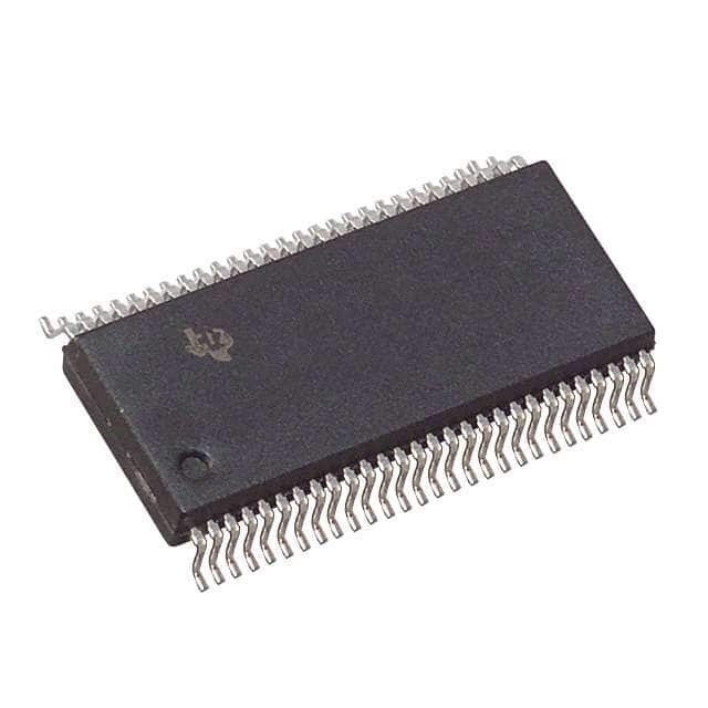
SN74ABT162501DLR
Product Overview
- Category: Integrated Circuit (IC)
- Use: Data Buffer/Driver
- Characteristics: High-speed, non-inverting, 16-bit bus buffer with 3-state outputs
- Package: 56-pin TSSOP (Thin Shrink Small Outline Package)
- Essence: The SN74ABT162501DLR is designed to provide buffering and driving capabilities for a 16-bit bus. It allows bidirectional transfer of data between different voltage domains or systems.
- Packaging/Quantity: The SN74ABT162501DLR is typically sold in reels containing 250 units.
Specifications
- Supply Voltage: 4.5V to 5.5V
- Input Voltage Levels: 0V to VCC
- Output Voltage Levels: 0V to VCC
- Operating Temperature Range: -40°C to +85°C
- Propagation Delay: 2.8ns (typical)
- Output Drive Capability: ±24mA
Detailed Pin Configuration
The SN74ABT162501DLR has a total of 56 pins. Here is the detailed pin configuration:
- OE (Output Enable) 1
- Y1 (Output) 1
- GND (Ground)
- Y2 (Output) 1
- Y3 (Output) 1
- Y4 (Output) 1
- Y5 (Output) 1
- Y6 (Output) 1
- Y7 (Output) 1
- Y8 (Output) 1
- Y9 (Output) 1
- Y10 (Output) 1
- Y11 (Output) 1
- Y12 (Output) 1
- VCC (Supply Voltage)
- Y13 (Output) 1
- Y14 (Output) 1
- Y15 (Output) 1
- Y16 (Output) 1
- GND (Ground)
- A1 (Input) 1
- B1 (Input) 1
- A2 (Input) 1
- B2 (Input) 1
- A3 (Input) 1
- B3 (Input) 1
- A4 (Input) 1
- B4 (Input) 1
- A5 (Input) 1
- B5 (Input) 1
- A6 (Input) 1
- B6 (Input) 1
- A7 (Input) 1
- B7 (Input) 1
- A8 (Input) 1
- B8 (Input) 1
- GND (Ground)
- A9 (Input) 1
- B9 (Input) 1
- A10 (Input) 1
- B10 (Input) 1
- A11 (Input) 1
- B11 (Input) 1
- A12 (Input) 1
- B12 (Input) 1
- A13 (Input) 1
- B13 (Input) 1
- A14 (Input) 1
- B14 (Input) 1
- A15 (Input) 1
- B15 (Input) 1
- A16 (Input) 1
- B16 (Input) 1
- GND (Ground)
- OE (Output Enable) 2
- Y1 (Output) 2
Functional Features
- Bidirectional data transfer between different voltage domains or systems.
- Non-inverting buffer with 3-state outputs.
- High-speed operation for efficient data transfer.
- Output enable control for easy interfacing with other devices.
Advantages and Disadvantages
Advantages: - Allows bidirectional data transfer, enhancing system flexibility. - High-speed operation enables efficient data processing. - 3-state outputs provide control over the bus lines. - Wide operating temperature range allows usage in various environments.
Disadvantages: - Limited output drive capability may not be suitable for high-current applications. - Requires careful consideration of voltage compatibility between input and output systems.
Working Principles
The SN74ABT162501DLR operates by receiving input data on its A1-A16 and B1-B16 pins. The data is then buffered and driven to the corresponding Y1-Y16 output pins. The direction of data transfer is controlled by the OE (Output Enable)
قم بإدراج 10 أسئلة وإجابات شائعة تتعلق بتطبيق SN74ABT162501DLR في الحلول التقنية
Sure! Here are 10 common questions and answers related to the application of SN74ABT162501DLR in technical solutions:
Q: What is SN74ABT162501DLR? A: SN74ABT162501DLR is a 16-bit bus transceiver with 3-state outputs, designed for high-speed digital systems.
Q: What is the operating voltage range of SN74ABT162501DLR? A: The operating voltage range is typically between 4.5V and 5.5V.
Q: What is the maximum data transfer rate supported by SN74ABT162501DLR? A: SN74ABT162501DLR supports a maximum data transfer rate of 250 MHz.
Q: Can SN74ABT162501DLR be used for bidirectional data communication? A: Yes, SN74ABT162501DLR can be used for bidirectional data communication as it has separate input and output ports.
Q: How many bits can SN74ABT162501DLR handle at a time? A: SN74ABT162501DLR is a 16-bit bus transceiver, meaning it can handle 16 bits of data simultaneously.
Q: Does SN74ABT162501DLR support 3-state outputs? A: Yes, SN74ABT162501DLR supports 3-state outputs, allowing multiple devices to share a common bus without interference.
Q: What is the typical propagation delay of SN74ABT162501DLR? A: The typical propagation delay of SN74ABT162501DLR is around 3.8 ns.
Q: Can SN74ABT162501DLR be used in high-speed applications? A: Yes, SN74ABT162501DLR is designed for high-speed digital systems and can be used in high-speed applications.
Q: Does SN74ABT162501DLR have built-in ESD protection? A: Yes, SN74ABT162501DLR has built-in ESD protection to prevent damage from electrostatic discharge.
Q: What package does SN74ABT162501DLR come in? A: SN74ABT162501DLR is available in a 56-pin TSSOP (Thin Shrink Small Outline Package) package.
Please note that the answers provided here are general and may vary depending on specific datasheet specifications and application requirements.


