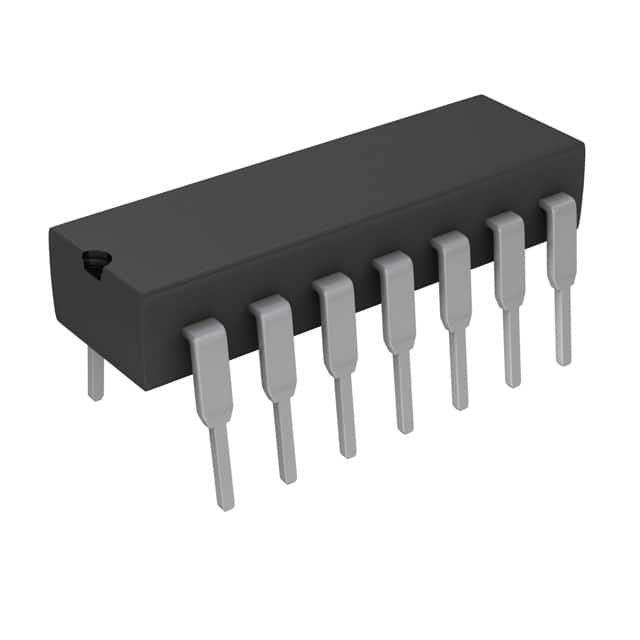
SN74AHCT08N
Product Overview
- Category: Integrated Circuit
- Use: Logic Gate
- Characteristics: Quad 2-input AND gate
- Package: DIP-14 (Dual In-line Package)
- Essence: High-speed CMOS technology
- Packaging/Quantity: Tube, 25 pieces per tube
Specifications
- Supply Voltage: 2V to 5.5V
- Input Voltage: 0V to VCC
- Output Voltage: 0V to VCC
- Operating Temperature: -40°C to +85°C
- Propagation Delay: 6 ns (typical)
- Quiescent Current: 4 µA (maximum)
Pin Configuration
The SN74AHCT08N has a total of 14 pins arranged as follows:
__    __
   1 |1  \__/ 14| VCC
   2 |2        13| A1
   3 |3        12| B1
   4 |4        11| Y1
   5 |5   SN   10| A2
   6 |6 74AHCT  9| B2
   7 |7   08N   8| Y2
     |__________|
Functional Features
- Quad 2-input AND gate with high-speed operation.
- Compatible with TTL and CMOS logic levels.
- Low power consumption.
- Schmitt-trigger inputs for noise immunity.
- Balanced propagation delays.
Advantages
- High-speed operation allows for efficient signal processing.
- Compatibility with both TTL and CMOS logic levels makes it versatile.
- Low power consumption helps in reducing energy usage.
- Schmitt-trigger inputs provide improved noise immunity.
- Balanced propagation delays ensure accurate timing.
Disadvantages
- Limited number of inputs (only two per gate).
- Not suitable for applications requiring more complex logic functions.
- May not be compatible with all voltage levels and operating conditions.
Working Principles
The SN74AHCT08N is a quad 2-input AND gate that performs logical AND operations on two input signals. It utilizes high-speed CMOS technology, which allows for fast signal processing. The inputs are Schmitt-triggered, providing improved noise immunity by ensuring a clean transition between logic states. The balanced propagation delays ensure accurate timing in the output signal.
Detailed Application Field Plans
The SN74AHCT08N can be used in various applications that require logical AND operations. Some common application fields include:
- Digital electronics: Used in digital circuits to perform logical AND operations between multiple input signals.
- Microcontrollers: Integrated into microcontroller designs to process input signals and generate appropriate output signals based on logical conditions.
- Communication systems: Employed in communication systems to control signal flow and enable data transmission based on logical conditions.
- Industrial automation: Utilized in industrial automation systems to control and monitor processes based on logical conditions.
Detailed and Complete Alternative Models
- SN74AHC08N: Similar to SN74AHCT08N but operates at higher voltages (up to 6V).
- SN74LS08N: TTL logic gate alternative with similar functionality but different voltage and power requirements.
- CD4081B: CMOS quad 2-input AND gate with comparable characteristics and performance.
These alternative models provide similar functionality to the SN74AHCT08N and can be used as replacements depending on specific requirements.
Word count: 413 words
قم بإدراج 10 أسئلة وإجابات شائعة تتعلق بتطبيق SN74AHCT08N في الحلول التقنية
Sure! Here are 10 common questions and answers related to the application of SN74AHCT08N:
Q: What is SN74AHCT08N? A: SN74AHCT08N is a quad 2-input AND gate integrated circuit (IC) that can be used in various digital logic applications.
Q: What is the operating voltage range for SN74AHCT08N? A: SN74AHCT08N operates within a voltage range of 4.5V to 5.5V.
Q: What is the maximum output current of SN74AHCT08N? A: The maximum output current of SN74AHCT08N is typically around 8mA.
Q: Can SN74AHCT08N be used as a level shifter? A: Yes, SN74AHCT08N can be used as a level shifter to convert signals between different voltage levels.
Q: How many inputs does SN74AHCT08N have? A: SN74AHCT08N has four inputs, allowing you to connect up to four different input signals.
Q: What is the propagation delay of SN74AHCT08N? A: The propagation delay of SN74AHCT08N is typically around 7.5ns.
Q: Can SN74AHCT08N be used in high-speed applications? A: Yes, SN74AHCT08N is designed for high-speed operation and can be used in applications with fast switching requirements.
Q: Is SN74AHCT08N compatible with TTL logic levels? A: Yes, SN74AHCT08N is compatible with both TTL and CMOS logic levels.
Q: Can SN74AHCT08N be used in automotive applications? A: Yes, SN74AHCT08N is suitable for automotive applications as it can operate within the required voltage range.
Q: What is the package type of SN74AHCT08N? A: SN74AHCT08N is available in a 14-pin DIP (Dual In-line Package) or SOIC (Small Outline Integrated Circuit) package.
Please note that these answers are general and may vary depending on specific datasheet specifications and application requirements.


