

SN74ALS874BNSRE4
Product Overview
- Category: Integrated Circuit (IC)
- Use: Logic Function
- Characteristics: High-speed, Low-power, TTL-Compatible
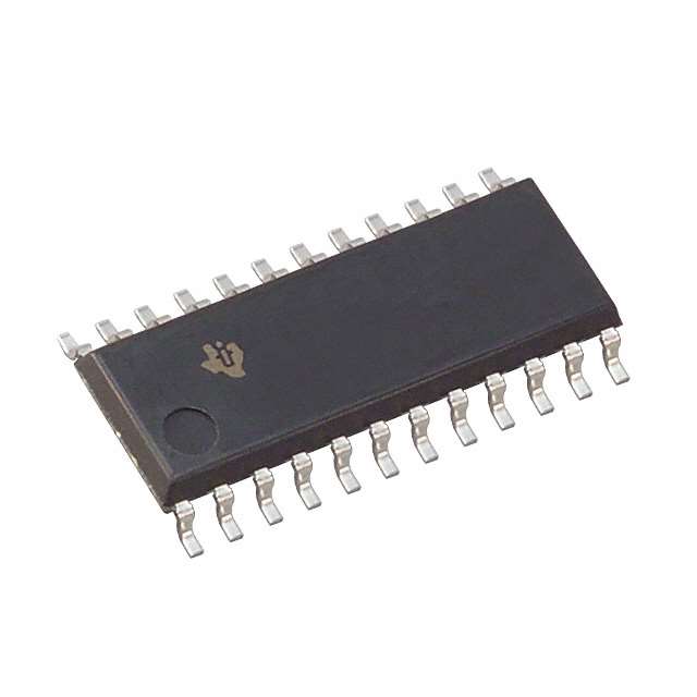
- Package: SOIC (Small Outline Integrated Circuit)
- Essence: 8-Bit D-Type Flip-Flop with 3-State Outputs
- Packaging/Quantity: Tape and Reel, 2500 units per reel
Specifications
- Supply Voltage Range: 4.5V to 5.5V
- Input Voltage Range: 0V to VCC
- Output Voltage Range: 0V to VCC
- Operating Temperature Range: -40°C to +85°C
- Propagation Delay Time: 7ns (typical)
- Output Current: ±24mA
- Input Capacitance: 3pF
- Output Capacitance: 15pF
Detailed Pin Configuration
The SN74ALS874BNSRE4 has a total of 20 pins. The pin configuration is as follows:
- CLR (Clear) - Active LOW clear input
- D0-D7 (Data Inputs) - Eight data inputs
- CP (Clock Pulse) - Clock pulse input
- OE (Output Enable) - Active LOW output enable input
- Q0-Q7 (Flip-Flop Outputs) - Eight flip-flop outputs
- GND (Ground) - Ground reference
- Q7' (Complementary Output) - Complementary output of Q7
- VCC (Supply Voltage) - Positive supply voltage
Functional Features
- 8-bit D-type flip-flop with 3-state outputs
- Synchronous operation with common clock
- Asynchronous active LOW clear
- 3-state outputs for bus-oriented applications
- TTL-compatible inputs and outputs
- High-speed operation with low power consumption
Advantages and Disadvantages
Advantages: - High-speed operation allows for efficient data processing - Low-power consumption helps in reducing energy usage - TTL-compatible inputs and outputs ensure compatibility with other logic devices - 3-state outputs enable bus-oriented applications
Disadvantages: - Limited operating temperature range (-40°C to +85°C) - Input and output voltage range limited to the supply voltage range (0V to VCC)
Working Principles
The SN74ALS874BNSRE4 is an 8-bit D-type flip-flop with 3-state outputs. It operates synchronously with a common clock pulse input (CP). The data inputs (D0-D7) are latched into the flip-flops on the rising edge of the clock pulse. The clear input (CLR) is asynchronous and active LOW, allowing for the clearing of all flip-flops when activated. The output enable input (OE) is active LOW and controls the 3-state outputs (Q0-Q7), enabling or disabling their functionality.
Detailed Application Field Plans
The SN74ALS874BNSRE4 is commonly used in various digital systems and applications, including:
- Microprocessors and microcontrollers
- Data storage systems
- Communication systems
- Industrial automation
- Automotive electronics
- Consumer electronics
Its high-speed operation, low-power consumption, and compatibility with TTL logic make it suitable for these applications.
Detailed and Complete Alternative Models
- SN74ALS876BNSRE4: 16-Bit D-Type Flip-Flop with 3-State Outputs
- SN74ALS872BNSRE4: 4-Bit D-Type Flip-Flop with 3-State Outputs
- SN74ALS878BNSRE4: 8-Bit Transparent Latch with 3-State Outputs
- SN74ALS870BNSRE4: Octal D-Type Transparent Latch with 3-State Outputs
These alternative models offer similar functionality and characteristics, providing options for different design requirements.
In conclusion, the SN74ALS874BNSRE4 is an 8-bit D-type flip-flop with 3-state outputs. It offers high-speed operation, low-power consumption, and compatibility with TTL logic. With its various applications and alternative models available, it serves as a versatile component in digital systems.
قم بإدراج 10 أسئلة وإجابات شائعة تتعلق بتطبيق SN74ALS874BNSRE4 في الحلول التقنية
Sure! Here are 10 common questions and answers related to the application of SN74ALS874BNSRE4 in technical solutions:
Q: What is SN74ALS874BNSRE4? A: SN74ALS874BNSRE4 is a specific model of integrated circuit (IC) that belongs to the ALS family of logic devices.
Q: What is the function of SN74ALS874BNSRE4? A: SN74ALS874BNSRE4 is an octal D-type transparent latch with 3-state outputs. It can store data and control the flow of information in a digital system.
Q: What is the operating voltage range for SN74ALS874BNSRE4? A: The operating voltage range for SN74ALS874BNSRE4 is typically between 4.5V and 5.5V.
Q: How many latches are there in SN74ALS874BNSRE4? A: SN74ALS874BNSRE4 has 8 individual latches, making it an octal latch.
Q: What is the maximum clock frequency supported by SN74ALS874BNSRE4? A: SN74ALS874BNSRE4 can operate at a maximum clock frequency of 25 MHz.
Q: Can SN74ALS874BNSRE4 be used in both parallel and serial data transfer applications? A: Yes, SN74ALS874BNSRE4 can be used in both parallel and serial data transfer applications, depending on the configuration and connection.
Q: What is the output drive capability of SN74ALS874BNSRE4? A: SN74ALS874BNSRE4 has a typical output drive capability of ±24 mA.
Q: Does SN74ALS874BNSRE4 have any built-in protection features? A: Yes, SN74ALS874BNSRE4 has built-in diode clamps to protect against electrostatic discharge (ESD) and other voltage spikes.
Q: Can SN74ALS874BNSRE4 be used in both commercial and industrial applications? A: Yes, SN74ALS874BNSRE4 is designed to operate reliably in both commercial and industrial temperature ranges.
Q: What are some typical applications of SN74ALS874BNSRE4? A: SN74ALS874BNSRE4 can be used in various applications such as data storage, address decoding, bus interfacing, and general-purpose digital logic circuits.
Please note that the answers provided here are general and may vary depending on the specific requirements and datasheet of SN74ALS874BNSRE4.