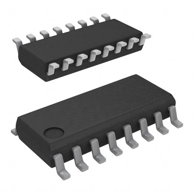
SN74AS109AD
Product Overview
- Category: Integrated Circuit (IC)
- Use: Digital Logic
- Characteristics: Dual J-K Flip-Flop with Clear
- Package: 16-pin DIP (Dual In-line Package)
- Essence: Flip-flop circuitry for storing and manipulating binary data
- Packaging/Quantity: Available in tubes or reels, quantity varies based on supplier
Specifications
- Supply Voltage Range: 4.5V to 5.5V
- High-Level Input Voltage: 2V
- Low-Level Input Voltage: 0.8V
- High-Level Output Voltage: 2.7V
- Low-Level Output Voltage: 0.5V
- Maximum Operating Frequency: 125 MHz
- Propagation Delay Time: 10 ns
- Operating Temperature Range: -40°C to +85°C
Detailed Pin Configuration
The SN74AS109AD has a total of 16 pins, which are assigned specific functions as follows:
- CLR (Clear) - Active LOW input for resetting the flip-flop.
- CLK (Clock) - Input for clock signal that triggers the flip-flop.
- J (J Input) - Input for setting the flip-flop output based on the clock signal.
- K (K Input) - Input for resetting the flip-flop output based on the clock signal.
- Q1 (Output 1) - Output for the first flip-flop.
- Q1̅ (Complementary Output 1) - Complementary output for the first flip-flop.
- GND (Ground) - Ground reference for the IC.
- Q2 (Output 2) - Output for the second flip-flop.
- Q2̅ (Complementary Output 2) - Complementary output for the second flip-flop.
- VCC (Positive Power Supply) - Positive power supply for the IC. 11-16. NC (No Connection) - These pins are not connected and are left unused.
Functional Features
The SN74AS109AD is a dual J-K flip-flop with clear functionality. It is designed to store and manipulate binary data in digital logic circuits. The flip-flop can be set or reset based on the clock signal and the inputs provided to the J and K pins. The clear input allows for resetting the flip-flop to a known state.
Advantages and Disadvantages
Advantages: - Dual flip-flop configuration allows for efficient storage and manipulation of binary data. - Clear functionality provides control over the initial state of the flip-flop. - Wide operating voltage range allows for compatibility with various digital systems. - High-speed operation enables quick data processing.
Disadvantages: - Limited number of flip-flops in a single package. - Requires external components for complete circuit implementation. - Propagation delay may affect timing-sensitive applications.
Working Principles
The SN74AS109AD operates based on the principles of J-K flip-flops. The J and K inputs determine the output state of the flip-flop when triggered by the clock signal. The clear input resets the flip-flop to a known state, typically all outputs set to 0. The flip-flop stores and retains its output state until a new clock signal triggers a change.
Detailed Application Field Plans
The SN74AS109AD finds application in various digital systems where binary data storage and manipulation are required. Some specific application areas include:
- Counters and Registers: The flip-flop can be used as building blocks for designing counters and registers in digital circuits.
- Sequential Logic Circuits: It is utilized in sequential logic circuits to store and process data based on clock signals.
- Data Synchronization: The flip-flop aids in synchronizing data between different parts of a digital system.
- State Machines: It is employed in the implementation of state machines for control and decision-making processes.
Detailed and Complete Alternative Models
- SN74AS109AN: Similar to SN74AS109AD, but available in a 14-pin DIP package.
- CD4013BE: Dual D-type flip-flop with clear, available in a 14-pin DIP package.
- MC14013B: Dual J-K flip-flop with set and reset, available in a 14-pin DIP package.
- 74HC109: Dual positive-edge triggered J-K flip-flop, available in various package options.
These alternative models provide similar functionality to the SN74AS109AD and can be used as replacements based on specific requirements.
In conclusion, the SN74AS109AD is a dual J-K flip-flop with clear functionality. It is widely used in digital logic circuits for storing and manipulating binary data. With its versatile applications and reliable performance, it serves as an essential component in various electronic systems.
قم بإدراج 10 أسئلة وإجابات شائعة تتعلق بتطبيق SN74AS109AD في الحلول التقنية
Sure! Here are 10 common questions and answers related to the application of SN74AS109AD in technical solutions:
Q: What is SN74AS109AD? A: SN74AS109AD is a dual J-K flip-flop integrated circuit (IC) that can be used in various digital applications.
Q: What is the purpose of using SN74AS109AD? A: SN74AS109AD is commonly used for storing and manipulating binary data in digital circuits, such as counters, registers, and frequency dividers.
Q: What is the maximum operating frequency of SN74AS109AD? A: The maximum operating frequency of SN74AS109AD is typically around 100 MHz.
Q: How many flip-flops are there in SN74AS109AD? A: SN74AS109AD consists of two independent J-K flip-flops.
Q: What is the power supply voltage range for SN74AS109AD? A: The power supply voltage range for SN74AS109AD is typically between 4.75V and 5.25V.
Q: Can SN74AS109AD be used in both positive-edge and negative-edge triggered systems? A: Yes, SN74AS109AD supports both positive-edge and negative-edge triggering, making it versatile for different system requirements.
Q: What is the output drive capability of SN74AS109AD? A: SN74AS109AD has a standard output drive capability, which means it can drive typical TTL loads.
Q: Does SN74AS109AD have any built-in asynchronous clear or preset inputs? A: No, SN74AS109AD does not have any built-in asynchronous clear or preset inputs.
Q: Can SN74AS109AD be cascaded to create larger counters or registers? A: Yes, SN74AS109AD can be cascaded with other flip-flops to create larger counters or registers.
Q: Are there any specific precautions to consider when using SN74AS109AD? A: It is important to ensure proper decoupling and bypass capacitors are used near the power supply pins of SN74AS109AD to minimize noise and voltage fluctuations.
Please note that the answers provided here are general and may vary depending on the specific application and requirements.


