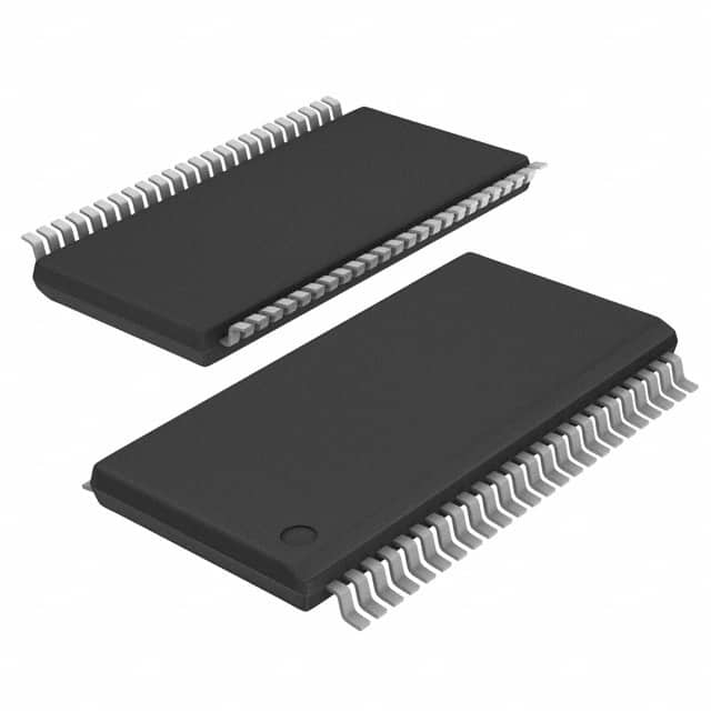
SN74AUC16240DGVR
Product Overview
- Category: Integrated Circuit
- Use: Buffer/Driver
- Characteristics: High-speed, low-power, voltage level shifting
- Package: VSSOP (Very Small Outline Package)
- Essence: Logic Level Translator
- Packaging/Quantity: Tape and Reel, 2500 pieces per reel
Specifications
- Supply Voltage Range: 0.8V to 3.6V
- Input Voltage Range: -0.5V to 5.5V
- Output Voltage Range: 0V to VCC
- Maximum Operating Frequency: 100 MHz
- Number of Channels: 16
- Output Drive Capability: ±24 mA
- Propagation Delay: 2.9 ns (typical)
Detailed Pin Configuration
The SN74AUC16240DGVR has a total of 48 pins, arranged in a VSSOP package. The pin configuration is as follows:
- OE#
- A1
- Y1
- A2
- Y2
- GND
- Y3
- A3
- Y4
- A4
- Y5
- A5
- Y6
- A6
- Y7
- A7
- Y8
- A8
- Y9
- A9
- Y10
- A10
- Y11
- A11
- Y12
- A12
- Y13
- A13
- Y14
- A14
- Y15
- A15
- Y16
- A16
- VCC
- B1
- Z1
- B2
- Z2
- GND
- Z3
- B3
- Z4
- B4
- Z5
- B5
- Z6
- B6
Functional Features
The SN74AUC16240DGVR is a high-speed buffer/driver IC that provides voltage level shifting capabilities. It is designed to interface between devices operating at different voltage levels, ensuring proper signal translation. The key features of this IC include:
- Wide supply voltage range, allowing compatibility with various systems.
- High-speed operation, enabling efficient data transmission.
- Low-power consumption, reducing energy requirements.
- 16 channels for simultaneous level shifting.
- Output drive capability of ±24 mA, ensuring strong signal integrity.
- Propagation delay of 2.9 ns (typical), minimizing signal latency.
Advantages and Disadvantages
Advantages: - Wide supply voltage range enables versatile usage. - High-speed operation facilitates fast data transfer. - Low-power consumption reduces energy costs. - Multiple channels allow for simultaneous level shifting. - Strong output drive capability ensures reliable signal transmission.
Disadvantages: - Limited maximum operating frequency compared to some other ICs. - VSSOP package may require careful handling during assembly.
Working Principles
The SN74AUC16240DGVR operates by receiving input signals from one voltage domain and translating them to the corresponding voltage level in another domain. It utilizes a combination of MOSFETs and CMOS technology to achieve efficient level shifting. The IC's internal circuitry ensures that the output signals accurately reflect the input signals, while maintaining high-speed operation and low power consumption.
Detailed Application Field Plans
The SN74AUC16240DGVR finds applications in various fields where voltage level translation is required. Some specific application areas include:
- Communication Systems: Used to interface between different voltage domains in communication devices such as routers, switches, and modems.
- Industrial Automation: Enables level shifting between control systems and sensors/actuators operating at different voltage levels.
- Automotive Electronics: Facilitates communication between various components in automotive systems, ensuring compatibility between different voltage domains.
- Consumer Electronics: Allows for proper signal translation between different subsystems in devices like smartphones, tablets, and gaming consoles.
Detailed and Complete Alternative Models
- SN74AUC16244DGVR: Similar to SN74AUC16240DGVR, but with 8 channels instead of 16.
- SN74LVC16240ADGGR: Offers similar functionality with a different package (TSSOP) and wider supply voltage range.
- SN74HCT244N: Provides level shifting capabilities with higher output drive capability and wider input voltage range.
These alternative models offer similar features and can be considered based on specific requirements and constraints.
Word count: 536 words
قم بإدراج 10 أسئلة وإجابات شائعة تتعلق بتطبيق SN74AUC16240DGVR في الحلول التقنية
Sure! Here are 10 common questions and answers related to the application of SN74AUC16240DGVR:
Q: What is SN74AUC16240DGVR? A: SN74AUC16240DGVR is a 16-bit buffer/driver with 3-state outputs, commonly used in digital logic applications.
Q: What is the operating voltage range for SN74AUC16240DGVR? A: The operating voltage range for SN74AUC16240DGVR is typically between 0.8V and 2.7V.
Q: What is the maximum output current that SN74AUC16240DGVR can drive? A: SN74AUC16240DGVR can drive up to 24mA of output current per channel.
Q: Can SN74AUC16240DGVR be used in bidirectional data transfer applications? A: No, SN74AUC16240DGVR is a unidirectional buffer/driver and does not support bidirectional data transfer.
Q: What is the propagation delay of SN74AUC16240DGVR? A: The typical propagation delay of SN74AUC16240DGVR is around 2.6ns.
Q: Can SN74AUC16240DGVR tolerate overvoltage on its inputs? A: Yes, SN74AUC16240DGVR has input voltage tolerance up to 3.6V, making it suitable for use in mixed-voltage systems.
Q: Is SN74AUC16240DGVR compatible with TTL and CMOS logic levels? A: Yes, SN74AUC16240DGVR is compatible with both TTL and CMOS logic levels.
Q: Can SN74AUC16240DGVR be used in high-speed applications? A: Yes, SN74AUC16240DGVR is designed for high-speed operation and can be used in applications with fast switching requirements.
Q: Does SN74AUC16240DGVR have built-in ESD protection? A: Yes, SN74AUC16240DGVR has built-in ESD protection on its inputs and outputs.
Q: What package options are available for SN74AUC16240DGVR? A: SN74AUC16240DGVR is available in various package options, such as VSSOP, TSSOP, and TVSOP, to suit different application requirements.
Please note that the answers provided here are general and may vary depending on the specific datasheet and manufacturer's specifications of SN74AUC16240DGVR.


