

SN74AUP1G126YFPR
Product Overview
- Category: Integrated Circuit
- Use: Logic Gate
- Characteristics: Single Bus Buffer Gate
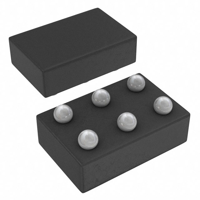
- Package: DSBGA (Dual Fine-Pitch Ball Grid Array)
- Essence: High-Speed CMOS Technology
- Packaging/Quantity: Tape and Reel, 3000 pieces per reel
Specifications
- Supply Voltage Range: 0.8V to 3.6V
- Input Voltage Range: 0V to VCC
- Output Voltage Range: 0V to VCC
- Maximum Operating Frequency: 500 MHz
- Propagation Delay: 2.5 ns (typical)
- Low Power Consumption: 0.9 µA (typical)
Detailed Pin Configuration
The SN74AUP1G126YFPR has the following pin configuration:
____
   Y1 |    | VCC
   A  |    | Y2
 GND  |____| OE
Functional Features
- Single bus buffer gate with output enable control
- Supports bidirectional data flow
- Provides high-speed signal buffering
- Compatible with various logic families
- Low power consumption for energy-efficient applications
Advantages
- Wide supply voltage range allows compatibility with different systems
- High operating frequency enables fast data processing
- Low propagation delay ensures minimal signal distortion
- Small package size saves board space
- Low power consumption extends battery life in portable devices
Disadvantages
- Limited number of input/output pins restricts complex circuit designs
- Sensitivity to electrostatic discharge requires proper handling precautions
- Higher cost compared to basic logic gates due to added functionality
Working Principles
The SN74AUP1G126YFPR is a single bus buffer gate that operates using high-speed CMOS technology. It acts as a signal amplifier and provides bidirectional data flow between the input (A) and output (Y1, Y2) pins. The output enable (OE) pin controls the buffer's operation, allowing the user to enable or disable the output.
Detailed Application Field Plans
The SN74AUP1G126YFPR is commonly used in various applications, including:
- Communication Systems: It facilitates signal buffering and level shifting in communication interfaces such as UART, SPI, and I2C.
- Microcontrollers: It serves as an interface between microcontrollers and peripheral devices, ensuring reliable data transfer.
- Memory Modules: It enables data buffering and signal conditioning in memory modules like RAM and Flash.
- Industrial Automation: It plays a vital role in controlling and monitoring industrial processes by interfacing sensors and actuators with control systems.
- Automotive Electronics: It is utilized in automotive systems for signal amplification and level translation in various modules like infotainment, powertrain, and body control units.
Detailed and Complete Alternative Models
- SN74AUP1G125DCKR
- SN74LVC1G126DBVR
- SN74AHC1G126DBVR
- SN74LVC1G126DCKR
- SN74LVC1G126YZPR
These alternative models offer similar functionality and can be considered as replacements for the SN74AUP1G126YFPR.
In conclusion, the SN74AUP1G126YFPR is a single bus buffer gate that provides high-speed signal buffering and bidirectional data flow. Its wide supply voltage range, low power consumption, and small package size make it suitable for various applications in communication systems, microcontrollers, memory modules, industrial automation, and automotive electronics. While it has limitations in terms of pin count and sensitivity to electrostatic discharge, there are alternative models available to suit different design requirements.
قم بإدراج 10 أسئلة وإجابات شائعة تتعلق بتطبيق SN74AUP1G126YFPR في الحلول التقنية
Sure! Here are 10 common questions and answers related to the application of SN74AUP1G126YFPR in technical solutions:
Q1: What is SN74AUP1G126YFPR? A1: SN74AUP1G126YFPR is a single bus buffer gate with 3-state output. It is a commonly used integrated circuit (IC) in electronic circuits.
Q2: What is the purpose of SN74AUP1G126YFPR? A2: SN74AUP1G126YFPR is used to buffer and control signals in digital circuits. It can be used to isolate different sections of a circuit or to interface between different voltage levels.
Q3: What is the voltage range supported by SN74AUP1G126YFPR? A3: SN74AUP1G126YFPR supports a voltage range from 0.8V to 3.6V, making it suitable for various low-power applications.
Q4: How many inputs and outputs does SN74AUP1G126YFPR have? A4: SN74AUP1G126YFPR has one input and one output. It is a single-channel device.
Q5: Can SN74AUP1G126YFPR handle bidirectional signals? A5: No, SN74AUP1G126YFPR is unidirectional and can only buffer signals in one direction.
Q6: What is the maximum data rate supported by SN74AUP1G126YFPR? A6: SN74AUP1G126YFPR can support data rates up to 400 Mbps, making it suitable for high-speed digital communication.
Q7: Is SN74AUP1G126YFPR compatible with other logic families? A7: Yes, SN74AUP1G126YFPR is compatible with a wide range of logic families, including TTL, CMOS, and LVCMOS.
Q8: Can SN74AUP1G126YFPR be used in battery-powered applications? A8: Yes, SN74AUP1G126YFPR is designed for low-power operation, making it suitable for battery-powered applications.
Q9: What is the package type of SN74AUP1G126YFPR? A9: SN74AUP1G126YFPR comes in a small footprint 5-pin SOT-23 package, which is commonly used in compact electronic designs.
Q10: Where can I find more information about the application of SN74AUP1G126YFPR? A10: You can refer to the datasheet provided by the manufacturer or visit their website for detailed application notes and examples.
Please note that the answers provided here are general and may vary depending on specific design requirements. It is always recommended to consult the datasheet and relevant technical documentation for accurate information.