

SN74AUP2G241DQER
Product Overview
Category
The SN74AUP2G241DQER belongs to the category of integrated circuits (ICs).
Use
This IC is commonly used in electronic devices for signal amplification and switching purposes.
Characteristics
- Low power consumption
- High-speed performance
- Wide operating voltage range
- Small form factor
- RoHS compliant
Package
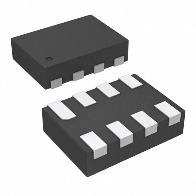
The SN74AUP2G241DQER is available in a small package, typically a dual-channel flip-flop with 8 pins.
Essence
The essence of this product lies in its ability to amplify and switch signals efficiently while consuming minimal power.
Packaging/Quantity
The SN74AUP2G241DQER is usually packaged in reels or tubes, with a quantity of 3000 units per reel/tube.
Specifications
- Supply Voltage: 1.65V to 3.6V
- Input Voltage Range: 0V to VCC
- Output Voltage Range: 0V to VCC
- Operating Temperature Range: -40°C to +85°C
- Maximum Propagation Delay: 4.5ns
- Maximum Power Dissipation: 500mW
Detailed Pin Configuration
The SN74AUP2G241DQER has the following pin configuration:
```
| | --| A | --| B | --| GND | --| Y | --| VCC | --| OE | --| | |___________| ```
Functional Features
- Dual-channel flip-flop functionality
- High-speed data transfer
- Low power consumption
- Schmitt-trigger inputs for noise immunity
- Output enable control for flexible operation
Advantages and Disadvantages
Advantages
- Low power consumption makes it suitable for battery-powered devices.
- High-speed performance enables efficient data transfer.
- Wide operating voltage range allows compatibility with various systems.
- Small form factor saves space in compact designs.
Disadvantages
- Limited number of channels compared to other ICs.
- May require additional components for certain applications.
- Sensitive to electrostatic discharge (ESD) and requires proper handling.
Working Principles
The SN74AUP2G241DQER operates based on the principles of digital logic. It uses flip-flops to store and manipulate binary data. The inputs control the state of the flip-flops, while the outputs provide the amplified or switched signals. The IC's internal circuitry ensures reliable operation within the specified voltage and temperature ranges.
Detailed Application Field Plans
The SN74AUP2G241DQER finds application in various electronic devices, including but not limited to: - Mobile phones - Tablets - Portable media players - Digital cameras - Gaming consoles
In these devices, it is used for signal amplification, level shifting, and data synchronization. Its small size and low power consumption make it ideal for portable and battery-powered devices.
Detailed and Complete Alternative Models
- SN74LVC2G241DCTR: Similar functionality with a wider operating voltage range.
- SN74HCT2G241DCUR: Higher speed performance with slightly higher power consumption.
- SN74LV2G241DCUR: Lower power consumption with reduced operating voltage range.
These alternative models offer similar features and can be considered as replacements for the SN74AUP2G241DQER depending on specific requirements.
Word count: 498 words
قم بإدراج 10 أسئلة وإجابات شائعة تتعلق بتطبيق SN74AUP2G241DQER في الحلول التقنية
Sure! Here are 10 common questions and answers related to the application of SN74AUP2G241DQER in technical solutions:
Question: What is the SN74AUP2G241DQER?
Answer: The SN74AUP2G241DQER is a dual buffer/driver with configurable voltage translation and integrated ESD protection.Question: What is the voltage range supported by SN74AUP2G241DQER?
Answer: The SN74AUP2G241DQER supports voltage translation from 0.8V to 3.6V.Question: Can I use the SN74AUP2G241DQER for level shifting between different voltage domains?
Answer: Yes, the SN74AUP2G241DQER is specifically designed for level shifting applications.Question: How many input/output pins does the SN74AUP2G241DQER have?
Answer: The SN74AUP2G241DQER has two input pins and two output pins.Question: What is the maximum data rate supported by SN74AUP2G241DQER?
Answer: The SN74AUP2G241DQER can support data rates up to 100 Mbps.Question: Does the SN74AUP2G241DQER have built-in ESD protection?
Answer: Yes, the SN74AUP2G241DQER has integrated ESD protection, making it suitable for robust applications.Question: Can I use the SN74AUP2G241DQER in battery-powered devices?
Answer: Yes, the SN74AUP2G241DQER has low power consumption, making it suitable for battery-powered applications.Question: Is the SN74AUP2G241DQER compatible with other logic families?
Answer: Yes, the SN74AUP2G241DQER is compatible with both CMOS and TTL logic families.Question: Can I use the SN74AUP2G241DQER in high-speed communication interfaces?
Answer: Yes, the SN74AUP2G241DQER can be used in various high-speed communication interfaces like UART, SPI, and I2C.Question: Are there any application notes or reference designs available for the SN74AUP2G241DQER?
Answer: Yes, Texas Instruments provides application notes and reference designs to help users implement the SN74AUP2G241DQER effectively in their designs.
Please note that these answers are general and may vary depending on specific design requirements. It's always recommended to refer to the datasheet and consult with technical experts for accurate information.