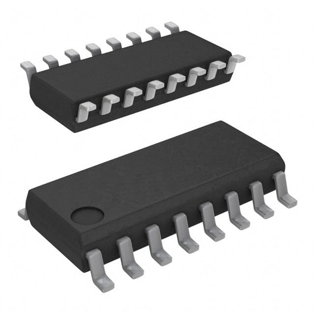
SN74F138DG4
Product Overview
Category
SN74F138DG4 belongs to the category of integrated circuits (ICs).
Use
This product is commonly used in digital electronics for decoding applications.
Characteristics
- High-speed operation
- Low power consumption
- Wide operating voltage range
- Multiple output enable inputs
- TTL-compatible inputs
Package
SN74F138DG4 is available in a 16-pin SOIC (Small Outline Integrated Circuit) package.
Essence
The essence of SN74F138DG4 lies in its ability to decode binary information and select one of the multiple outputs based on the input signals.
Packaging/Quantity
SN74F138DG4 is typically packaged in reels or tubes, with each reel containing 2500 units.
Specifications
- Supply Voltage: 2V to 6V
- Input Voltage: 0V to VCC
- Output Voltage: 0V to VCC
- Operating Temperature Range: -40°C to +85°C
- Maximum Propagation Delay: 18ns
Detailed Pin Configuration
- GND (Ground)
- A0 (Input A0)
- A1 (Input A1)
- A2 (Input A2)
- /G1 (Enable Input G1)
- /G2A (Enable Input G2A)
- /G2B (Enable Input G2B)
- Y0 (Output Y0)
- Y1 (Output Y1)
- Y2 (Output Y2)
- Y3 (Output Y3)
- VCC (Supply Voltage)
Functional Features
SN74F138DG4 is a 3-to-8 line decoder/demultiplexer. It takes three binary inputs (A0, A1, A2) and generates eight mutually exclusive outputs (Y0-Y7) based on the input combination. The enable inputs (/G1, /G2A, /G2B) control the operation of the decoder.
Advantages and Disadvantages
Advantages
- High-speed operation allows for quick decoding of input signals.
- Low power consumption makes it suitable for battery-powered devices.
- Wide operating voltage range provides flexibility in various applications.
- Multiple output enable inputs offer enhanced control over the decoder's functionality.
- TTL-compatible inputs ensure compatibility with other digital logic circuits.
Disadvantages
- Limited to 3-to-8 line decoding, not suitable for larger decoding requirements.
- Propagation delay of 18ns may introduce timing issues in certain high-speed applications.
Working Principles
SN74F138DG4 works on the principle of combinational logic. The binary inputs (A0, A1, A2) are decoded to select one of the eight outputs (Y0-Y7). The enable inputs (/G1, /G2A, /G2B) control the activation of the decoder. When the appropriate input combination is applied, the corresponding output becomes active.
Detailed Application Field Plans
SN74F138DG4 finds applications in various fields, including: 1. Address decoding in microprocessors and memory systems. 2. Data routing and selection in multiplexers and demultiplexers. 3. Control signal generation in digital systems. 4. Code conversion in binary-to-decimal or decimal-to-binary converters. 5. Logic circuit design and implementation.
Detailed and Complete Alternative Models
Some alternative models that can be considered as alternatives to SN74F138DG4 are: 1. 74HC138: A CMOS version of the decoder with similar functionality. 2. CD74HCT138: A high-speed TTL-compatible decoder with improved noise immunity. 3. SN54LS138: A low-power Schottky TTL decoder with comparable features.
These alternative models provide similar decoding capabilities and can be used as substitutes depending on specific requirements.
Word count: 511 words
قم بإدراج 10 أسئلة وإجابات شائعة تتعلق بتطبيق SN74F138DG4 في الحلول التقنية
Sure! Here are 10 common questions and answers related to the application of SN74F138DG4:
Q: What is SN74F138DG4? A: SN74F138DG4 is a 3-to-8 line decoder/demultiplexer integrated circuit (IC) manufactured by Texas Instruments.
Q: What is the purpose of SN74F138DG4? A: SN74F138DG4 is used to decode binary information from a microcontroller or other digital device into multiple output lines.
Q: How many input lines does SN74F138DG4 have? A: SN74F138DG4 has three input lines (A0, A1, and A2) that can be used to select one of the eight output lines.
Q: What is the maximum operating voltage for SN74F138DG4? A: The maximum operating voltage for SN74F138DG4 is 5.5 volts.
Q: Can SN74F138DG4 be used with both TTL and CMOS logic levels? A: Yes, SN74F138DG4 is compatible with both TTL and CMOS logic levels.
Q: What is the maximum output current of SN74F138DG4? A: The maximum output current of SN74F138DG4 is 24 mA.
Q: Can SN74F138DG4 be cascaded to increase the number of output lines? A: Yes, multiple SN74F138DG4 ICs can be cascaded together to increase the number of output lines.
Q: What is the typical propagation delay of SN74F138DG4? A: The typical propagation delay of SN74F138DG4 is around 10 ns.
Q: Can SN74F138DG4 be used in both active-high and active-low configurations? A: Yes, SN74F138DG4 can be used in both active-high and active-low configurations depending on the input signals.
Q: What are some common applications of SN74F138DG4? A: SN74F138DG4 is commonly used in address decoding, memory selection, data routing, and general-purpose digital logic circuits.
Please note that these answers are general and may vary depending on specific application requirements and datasheet specifications.


