

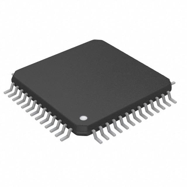
SN74FB2040RCG3
Product Overview
- Category: Integrated Circuit
- Use: Logic Gate
- Characteristics: High-speed, Low-power consumption
- Package: QFN (Quad Flat No-leads)
- Essence: Digital Logic IC
- Packaging/Quantity: Tape and Reel, 2500 units per reel
Specifications
- Supply Voltage: 1.65V to 3.6V
- Logic Family: FB (Fast Buffer)
- Number of Inputs: 4
- Number of Outputs: 4
- Propagation Delay: 2.5ns (typical)
- Operating Temperature Range: -40°C to +85°C
Detailed Pin Configuration
The SN74FB2040RCG3 has a total of 16 pins arranged as follows:
___________
       |           |
   VCC |1         16| GND
   A1  |2         15| B1
   A2  |3         14| B2
   Y1  |4         13| Y2
   A3  |5         12| B3
   A4  |6         11| B4
   Y3  |7         10| Y4
   OE  |8          9| NC
       |___________|
Functional Features
- The SN74FB2040RCG3 is a quad 2-input NOR gate.
- It operates at high speed with low power consumption.
- The device has an output enable (OE) pin for easy control of the outputs.
- It provides a wide operating voltage range, making it suitable for various applications.
Advantages and Disadvantages
Advantages: - High-speed operation allows for efficient data processing. - Low-power consumption reduces energy usage. - Wide operating voltage range enhances versatility. - Output enable pin provides flexibility in controlling the outputs.
Disadvantages: - Limited number of inputs and outputs restricts complex logic operations. - Propagation delay may affect timing-sensitive applications.
Working Principles
The SN74FB2040RCG3 operates based on the principles of digital logic. It uses NOR gates to perform logical operations on input signals. The device combines multiple NOR gates into a single integrated circuit, allowing for compact and efficient implementation of logic functions. The inputs are processed internally, and the resulting output is determined by the logic operation performed by the NOR gates.
Detailed Application Field Plans
The SN74FB2040RCG3 can be used in various applications, including:
Microprocessor Systems: The device can be utilized in microprocessor-based systems for performing logical operations and interfacing with other components.
Communication Systems: It can be employed in communication systems for signal processing and data manipulation.
Industrial Control Systems: The IC can be integrated into industrial control systems to implement logic functions required for process control and automation.
Consumer Electronics: The device finds application in consumer electronics such as TVs, audio systems, and gaming consoles for logic operations and signal processing.
Detailed and Complete Alternative Models
- SN74FB2041RCG3: Similar to SN74FB2040RCG3 but with 8 inputs and 8 outputs.
- SN74FB2042RCG3: Similar to SN74FB2040RCG3 but with 2 inputs and 2 outputs.
- SN74FB2043RCG3: Similar to SN74FB2040RCG3 but with 3 inputs and 3 outputs.
- SN74FB2044RCG3: Similar to SN74FB2040RCG3 but with 4 inputs and 4 outputs.
These alternative models provide options with different input/output configurations to suit specific application requirements.
Word count: 372 words
قم بإدراج 10 أسئلة وإجابات شائعة تتعلق بتطبيق SN74FB2040RCG3 في الحلول التقنية
Sure! Here are 10 common questions and answers related to the application of SN74FB2040RCG3 in technical solutions:
Q: What is SN74FB2040RCG3? A: SN74FB2040RCG3 is a specific model of integrated circuit (IC) manufactured by Texas Instruments.
Q: What is the purpose of SN74FB2040RCG3? A: SN74FB2040RCG3 is a high-speed, low-power buffer and level shifter IC designed for use in various digital applications.
Q: What voltage levels does SN74FB2040RCG3 support? A: SN74FB2040RCG3 supports voltage level translation between 1.2V and 3.3V.
Q: Can SN74FB2040RCG3 be used for bidirectional level shifting? A: Yes, SN74FB2040RCG3 supports bidirectional level shifting, allowing translation from one voltage domain to another.
Q: What is the maximum data rate supported by SN74FB2040RCG3? A: SN74FB2040RCG3 can handle data rates up to 100 Mbps.
Q: Is SN74FB2040RCG3 compatible with different logic families? A: Yes, SN74FB2040RCG3 is compatible with various logic families such as CMOS, TTL, and LVCMOS.
Q: Can SN74FB2040RCG3 be used in automotive applications? A: Yes, SN74FB2040RCG3 is qualified for automotive applications and meets the necessary standards.
Q: Does SN74FB2040RCG3 have built-in ESD protection? A: Yes, SN74FB2040RCG3 incorporates built-in ESD protection to safeguard against electrostatic discharge.
Q: What is the operating temperature range of SN74FB2040RCG3? A: SN74FB2040RCG3 can operate within a temperature range of -40°C to +125°C.
Q: Are there any application examples for SN74FB2040RCG3? A: Yes, SN74FB2040RCG3 can be used in various applications such as level shifting between different voltage domains, interfacing microcontrollers with different logic levels, and signal translation in communication systems.
Please note that these answers are general and may vary depending on the specific requirements and use cases. It's always recommended to refer to the datasheet and consult with technical experts for accurate information.