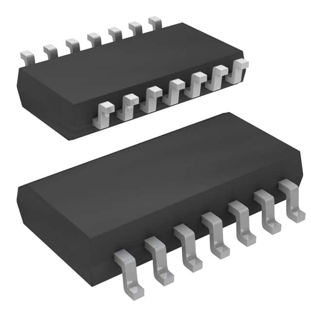
SN74LV125ATNSE4
Product Overview
Category
SN74LV125ATNSE4 belongs to the category of integrated circuits (ICs).
Use
It is commonly used as a quad buffer/line driver with 3-state outputs.
Characteristics
- Low-voltage operation: operates at a voltage range of 1.65V to 5.5V.
- High-speed performance: provides fast data transmission.
- 3-state outputs: allows multiple devices to share a common bus.
- Schmitt-trigger inputs: ensures noise immunity and signal integrity.
- Wide operating temperature range: can operate in various environmental conditions.
Package
SN74LV125ATNSE4 is available in a small-sized package, such as TSSOP or DGG.
Essence
The essence of SN74LV125ATNSE4 lies in its ability to buffer and drive signals while maintaining compatibility with different voltage levels.
Packaging/Quantity
Typically, SN74LV125ATNSE4 is packaged in reels or tubes, containing a specific quantity of ICs per package.
Specifications
- Supply Voltage Range: 1.65V to 5.5V
- Input Voltage Range: 0V to VCC
- Output Voltage Range: 0V to VCC
- Operating Temperature Range: -40°C to +85°C
- Logic Family: LV
- Number of Channels: 4
- Output Type: 3-state
Detailed Pin Configuration
SN74LV125ATNSE4 has a total of 14 pins, which are assigned specific functions:
- GND: Ground reference for the IC.
- A1: Input pin for channel 1.
- Y1: Output pin for channel 1.
- OE1: Output enable pin for channel 1.
- A2: Input pin for channel 2.
- Y2: Output pin for channel 2.
- OE2: Output enable pin for channel 2.
- VCC: Positive supply voltage.
- A3: Input pin for channel 3.
- Y3: Output pin for channel 3.
- OE3: Output enable pin for channel 3.
- A4: Input pin for channel 4.
- Y4: Output pin for channel 4.
- OE4: Output enable pin for channel 4.
Functional Features
SN74LV125ATNSE4 offers the following functional features:
- Buffering and line driving: It can buffer and drive signals, ensuring signal integrity and compatibility with different devices.
- 3-state outputs: The 3-state outputs allow multiple devices to share a common bus, enabling efficient data transmission.
- Schmitt-trigger inputs: The Schmitt-trigger inputs provide noise immunity, making it suitable for noisy environments.
- Low-voltage operation: It operates at low voltages, making it compatible with various power supply systems.
Advantages and Disadvantages
Advantages
- Wide operating voltage range allows compatibility with different systems.
- High-speed performance enables fast data transmission.
- 3-state outputs facilitate efficient sharing of a common bus.
- Schmitt-trigger inputs ensure noise immunity and signal integrity.
- Small package size makes it suitable for space-constrained applications.
Disadvantages
- Limited number of channels (4) may not be sufficient for certain applications requiring more inputs/outputs.
- Lack of built-in protection features against overvoltage or ESD events.
Working Principles
SN74LV125ATNSE4 operates based on the principles of buffering and line driving. It takes input signals from the A1-A4 pins and buffers them to the corresponding Y1-Y4 output pins. The OE1-OE4 pins control the output enable function, allowing the user to enable or disable the outputs as needed. The IC operates within the specified voltage range and uses Schmitt-trigger inputs to ensure noise immunity and signal integrity.
Detailed Application Field Plans
SN74LV125ATNSE4 finds applications in various fields, including:
- Communication systems: It can be used for buffering and driving signals in communication interfaces, such as UART, SPI, or I2C.
- Industrial automation: It is suitable for controlling and interfacing with sensors, actuators, and other devices in industrial automation systems.
- Automotive electronics: SN74LV125ATNSE4 can be utilized in automotive applications, such as vehicle control units, infotainment systems, and sensor interfaces.
- Consumer electronics: It finds use in consumer electronic devices like smartphones, tablets, and gaming consoles for signal buffering and driving purposes.
Detailed and Complete Alternative Models
Some alternative models that offer similar functionality to SN74LV125ATNSE4 are:
- SN74LVC125A: This IC offers similar features but operates at a wider voltage range of 1.65V to 3
قم بإدراج 10 أسئلة وإجابات شائعة تتعلق بتطبيق SN74LV125ATNSE4 في الحلول التقنية
Sure! Here are 10 common questions and answers related to the application of SN74LV125ATNSE4 in technical solutions:
Q: What is SN74LV125ATNSE4? A: SN74LV125ATNSE4 is a quad bus buffer gate with 3-state outputs, which means it can be used to amplify and buffer digital signals.
Q: What is the voltage range supported by SN74LV125ATNSE4? A: SN74LV125ATNSE4 supports a voltage range from 1.65V to 5.5V.
Q: How many channels does SN74LV125ATNSE4 have? A: SN74LV125ATNSE4 has four independent channels, allowing you to buffer up to four different signals.
Q: Can SN74LV125ATNSE4 be used for level shifting? A: Yes, SN74LV125ATNSE4 can be used for level shifting as it supports both low-voltage and high-voltage applications.
Q: What is the maximum output current of SN74LV125ATNSE4? A: The maximum output current per channel of SN74LV125ATNSE4 is 12mA.
Q: Is SN74LV125ATNSE4 compatible with standard CMOS logic levels? A: Yes, SN74LV125ATNSE4 is compatible with standard CMOS logic levels, making it suitable for various digital applications.
Q: Can SN74LV125ATNSE4 be used in bidirectional applications? A: No, SN74LV125ATNSE4 is not designed for bidirectional applications. It is a unidirectional buffer gate.
Q: What is the propagation delay of SN74LV125ATNSE4? A: The typical propagation delay of SN74LV125ATNSE4 is around 5.8ns.
Q: Does SN74LV125ATNSE4 have built-in ESD protection? A: Yes, SN74LV125ATNSE4 has built-in ESD protection, which helps protect the device from electrostatic discharge.
Q: What package options are available for SN74LV125ATNSE4? A: SN74LV125ATNSE4 is available in various package options, including SOIC, TSSOP, and VQFN, providing flexibility for different PCB designs.
Please note that these answers are general and may vary depending on the specific datasheet and application requirements.


