

SN74LVC126ARGYR
Product Overview
- Category: Integrated Circuit (IC)
- Use: Buffer/Driver
- Characteristics: Low-voltage, high-speed, non-inverting
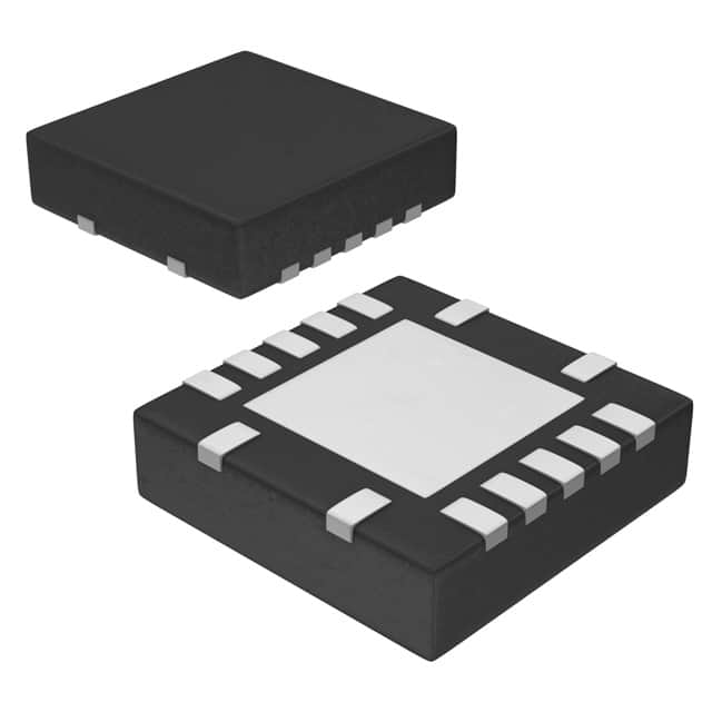
- Package: 14-pin VQFN package
- Essence: Logic gate with four independent buffer/driver channels
- Packaging/Quantity: Tape and reel packaging, 2500 units per reel
Specifications
- Supply Voltage Range: 1.65V to 5.5V
- High-Level Input Voltage: 2.3V to VCC
- Low-Level Input Voltage: GND to 0.8V
- High-Level Output Voltage: VCC - 0.4V
- Low-Level Output Voltage: 0.4V
- Maximum Operating Frequency: 400MHz
- Propagation Delay Time: 2.6ns (typical)
Detailed Pin Configuration
The SN74LVC126ARGYR has a 14-pin VQFN package with the following pin configuration:
- OE (Output Enable) for Channel 1
- A1 (Input) for Channel 1
- Y1 (Output) for Channel 1
- GND (Ground)
- Y2 (Output) for Channel 2
- A2 (Input) for Channel 2
- VCC (Supply Voltage)
- B2 (Input) for Channel 2
- OE (Output Enable) for Channel 2
- B1 (Input) for Channel 1
- Y3 (Output) for Channel 3
- A3 (Input) for Channel 3
- B3 (Input) for Channel 3
- OE (Output Enable) for Channel 3
Functional Features
- Non-inverting buffer/driver with 3-state outputs
- Independent control of each channel's output enable (OE) pin
- High-speed operation suitable for various applications
- Low-voltage operation allows compatibility with different logic levels
- 3-state outputs provide flexibility in connecting multiple devices
Advantages and Disadvantages
Advantages: - High-speed operation enables efficient data transfer - Low-voltage operation reduces power consumption - Independent control of each channel allows flexible usage - 3-state outputs facilitate bus sharing and multiplexing
Disadvantages: - Limited number of channels (4 in total) - Not suitable for high-power applications
Working Principles
The SN74LVC126ARGYR is a buffer/driver IC that amplifies and controls the signals passing through its input pins. It operates on a low supply voltage range of 1.65V to 5.5V, making it compatible with various logic levels. The non-inverting nature of the device ensures that the output signal matches the input signal.
The independent control of each channel's output enable (OE) pin allows the user to selectively enable or disable specific channels as needed. This feature provides flexibility in connecting multiple devices and facilitates bus sharing and multiplexing.
Detailed Application Field Plans
The SN74LVC126ARGYR can be used in various applications, including:
- Data communication systems: The high-speed operation and low-voltage capability make it suitable for use in data transmission and reception circuits.
- Microcontroller interfacing: The buffer/driver can be used to interface microcontrollers with other devices, such as sensors, actuators, and displays.
- Memory address decoding: The IC can be employed in memory address decoding circuits to select specific memory locations.
- Bus driving: The 3-state outputs allow the device to drive buses efficiently, enabling communication between multiple devices.
Detailed and Complete Alternative Models
- SN74LVC126A: Similar to SN74LVC126ARGYR, but available in different package options.
- SN74LVC125A: Quad buffer/driver with 3-state outputs, suitable for similar applications.
- SN74LVC244A: Octal buffer/driver with 3-state outputs, offering more channels for larger-scale applications.
These alternative models provide similar functionality and can be considered based on specific requirements and availability.
Word count: 536 words
قم بإدراج 10 أسئلة وإجابات شائعة تتعلق بتطبيق SN74LVC126ARGYR في الحلول التقنية
Sure! Here are 10 common questions and answers related to the application of SN74LVC126ARGYR:
Q: What is SN74LVC126ARGYR? A: SN74LVC126ARGYR is a quad buffer gate with 3-state outputs, commonly used in digital logic circuits.
Q: What is the operating voltage range for SN74LVC126ARGYR? A: The operating voltage range for SN74LVC126ARGYR is typically between 1.65V and 5.5V.
Q: What is the maximum output current that SN74LVC126ARGYR can drive? A: SN74LVC126ARGYR can drive up to 32mA of output current per channel.
Q: Can SN74LVC126ARGYR be used as a level shifter? A: Yes, SN74LVC126ARGYR can be used as a level shifter to convert signals between different voltage levels.
Q: How many channels does SN74LVC126ARGYR have? A: SN74LVC126ARGYR has four independent buffer gates, each with its own input and output.
Q: What is the propagation delay of SN74LVC126ARGYR? A: The typical propagation delay of SN74LVC126ARGYR is around 3.8ns.
Q: Can SN74LVC126ARGYR be used in high-speed applications? A: Yes, SN74LVC126ARGYR is designed for high-speed operation and can be used in applications with fast switching requirements.
Q: Is SN74LVC126ARGYR compatible with both CMOS and TTL logic levels? A: Yes, SN74LVC126ARGYR is compatible with both CMOS and TTL logic levels.
Q: Can SN74LVC126ARGYR be used in bidirectional applications? A: No, SN74LVC126ARGYR is a unidirectional buffer gate and cannot be used for bidirectional communication.
Q: What is the package type of SN74LVC126ARGYR? A: SN74LVC126ARGYR is available in a small-outline integrated circuit (SOIC) package.
Please note that these answers are general and may vary depending on specific datasheet specifications and application requirements.