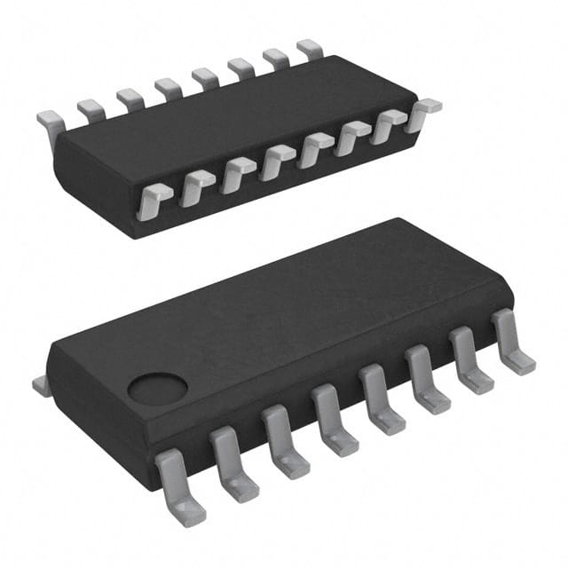
SN74LVC138AQDRG4Q1
Product Overview
- Category: Integrated Circuit (IC)
- Use: Decoder/Demultiplexer
- Characteristics: Low-Voltage CMOS Logic, Automotive-Qualified
- Package: 16-pin SOIC (Small Outline Integrated Circuit)
- Essence: High-performance decoder/demultiplexer for automotive applications
- Packaging/Quantity: Tape and Reel, 2500 units per reel
Specifications
- Supply Voltage Range: 1.65V to 5.5V
- Input Voltage Range: 0V to VCC
- Output Voltage Range: 0V to VCC
- Maximum Operating Frequency: 100 MHz
- Number of Outputs: 8
- Propagation Delay Time: 3.7 ns (typical)
- Operating Temperature Range: -40°C to +125°C
Detailed Pin Configuration
The SN74LVC138AQDRG4Q1 has a total of 16 pins. The pin configuration is as follows:
- GND (Ground)
- A0 (Address Input 0)
- A1 (Address Input 1)
- A2 (Address Input 2)
- /E1 (Enable Input 1, active low)
- Y0 (Output 0)
- Y1 (Output 1)
- Y2 (Output 2)
- Y3 (Output 3)
- /E2 (Enable Input 2, active low)
- Y4 (Output 4)
- Y5 (Output 5)
- Y6 (Output 6)
- Y7 (Output 7)
- VCC (Supply Voltage)
- GND (Ground)
Functional Features
- Decodes 3-bit binary-coded inputs into 8 mutually exclusive outputs
- Low-voltage CMOS technology for reduced power consumption
- Automotive-qualified, suitable for use in automotive applications
- High-speed operation with a maximum frequency of 100 MHz
- Wide supply voltage range allows compatibility with various systems
Advantages and Disadvantages
Advantages: - Low power consumption due to CMOS technology - Automotive qualification ensures reliability in harsh environments - High-speed operation enables efficient data processing - Wide supply voltage range provides flexibility in system design
Disadvantages: - Limited number of outputs (8) - Propagation delay time may affect timing-sensitive applications
Working Principles
The SN74LVC138AQDRG4Q1 is a decoder/demultiplexer IC that takes a 3-bit binary-coded input and generates 8 mutually exclusive outputs. The inputs A0, A1, and A2 determine which output is active based on the binary value applied. The enable inputs (/E1 and /E2) control the overall operation of the device.
When the enable input (/E1) is low, the outputs Y0 to Y7 are enabled, and the selected output is determined by the binary input. When the enable input (/E2) is low, the outputs Y0 to Y7 are disabled regardless of the binary input.
Detailed Application Field Plans
The SN74LVC138AQDRG4Q1 is specifically designed for automotive applications where decoding and demultiplexing functions are required. It can be used in various automotive systems such as:
- Infotainment Systems: Decoding audio/video signals for display and audio processing.
- Lighting Control: Demultiplexing control signals for controlling different lighting elements in the vehicle.
- Sensor Interface: Decoding sensor inputs for monitoring various parameters like temperature, pressure, etc.
- Communication Systems: Demultiplexing data signals for communication between different modules in the vehicle.
Detailed and Complete Alternative Models
- SN74LVC138A: Non-automotive version of the SN74LVC138AQDRG4Q1.
- 74HC138: High-speed CMOS version with similar functionality.
- CD74HC138: High-speed CMOS version from a different manufacturer.
These alternative models offer similar decoding/demultiplexing functionality but may have different characteristics, package options, or operating temperature ranges.
Word count: 452 words
قم بإدراج 10 أسئلة وإجابات شائعة تتعلق بتطبيق SN74LVC138AQDRG4Q1 في الحلول التقنية
Sure! Here are 10 common questions and answers related to the application of SN74LVC138AQDRG4Q1 in technical solutions:
1. What is SN74LVC138AQDRG4Q1? SN74LVC138AQDRG4Q1 is a 3-to-8 line decoder/demultiplexer IC (integrated circuit) that is commonly used in digital electronics applications.
2. What is the purpose of SN74LVC138AQDRG4Q1? The purpose of SN74LVC138AQDRG4Q1 is to decode a binary input and select one of the eight output lines based on the input value.
3. What voltage levels does SN74LVC138AQDRG4Q1 support? SN74LVC138AQDRG4Q1 supports voltage levels from 1.65V to 5.5V, making it compatible with a wide range of digital systems.
4. How many inputs does SN74LVC138AQDRG4Q1 have? SN74LVC138AQDRG4Q1 has three binary inputs (A0, A1, and A2) that determine which output line is selected.
5. How many output lines does SN74LVC138AQDRG4Q1 have? SN74LVC138AQDRG4Q1 has eight output lines (Y0-Y7), allowing for the selection of one out of the eight possible combinations of the input values.
6. Can SN74LVC138AQDRG4Q1 be cascaded to increase the number of output lines? Yes, multiple SN74LVC138AQDRG4Q1 ICs can be cascaded together to increase the number of output lines and decode larger binary numbers.
7. What is the maximum frequency at which SN74LVC138AQDRG4Q1 can operate? SN74LVC138AQDRG4Q1 can operate at a maximum frequency of 100 MHz, making it suitable for high-speed digital applications.
8. Is SN74LVC138AQDRG4Q1 compatible with both CMOS and TTL logic levels? Yes, SN74LVC138AQDRG4Q1 is compatible with both CMOS (Complementary Metal-Oxide-Semiconductor) and TTL (Transistor-Transistor Logic) logic levels.
9. What is the power supply voltage range for SN74LVC138AQDRG4Q1? The power supply voltage range for SN74LVC138AQDRG4Q1 is from 1.65V to 5.5V.
10. Can SN74LVC138AQDRG4Q1 be used in automotive applications? Yes, SN74LVC138AQDRG4Q1 is specifically designed for automotive applications and is qualified for use in automotive systems.
Please note that these answers are general and may vary depending on specific application requirements. It is always recommended to refer to the datasheet and consult with technical experts for accurate information.


