

SN74LVC1G10YZPR
Product Overview
Category
The SN74LVC1G10YZPR belongs to the category of integrated circuits (ICs).
Use
This IC is commonly used as a triple 3-input NAND gate.
Characteristics
- Low-voltage CMOS technology
- High-speed operation
- Low power consumption
- Schmitt-trigger inputs for noise immunity
- Wide operating voltage range
- Small package size
Package
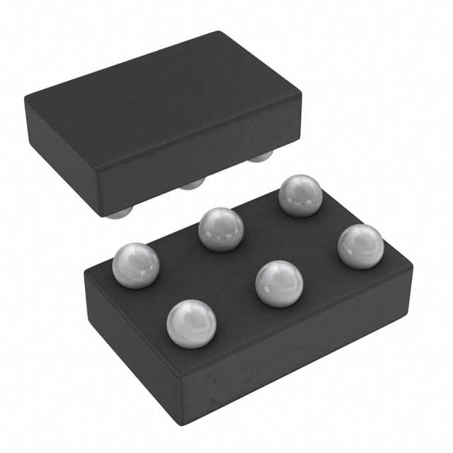
The SN74LVC1G10YZPR is available in a small-sized package, typically a 5-pin SOT-23 package.
Essence
The essence of this product lies in its ability to perform logic operations using three input signals and providing an output based on the NAND gate truth table.
Packaging/Quantity
The SN74LVC1G10YZPR is usually packaged in reels or tubes, with a quantity of 3000 units per reel/tube.
Specifications
- Supply Voltage: 1.65V to 5.5V
- Input Voltage Range: 0V to VCC
- Output Voltage Range: 0V to VCC
- Operating Temperature Range: -40°C to +85°C
- Propagation Delay Time: 4.2ns (typical) at 3.3V supply voltage
Detailed Pin Configuration
The SN74LVC1G10YZPR has the following pin configuration:
____
   A --|    |
   B --|    |
   C --|    |
 GND --|    |
   Y --|____|
Functional Features
- Triple 3-input NAND gate functionality
- Schmitt-trigger inputs for improved noise immunity
- Wide operating voltage range allows compatibility with various systems
- High-speed operation enables quick signal processing
- Low power consumption for energy-efficient applications
Advantages and Disadvantages
Advantages
- Low-voltage CMOS technology provides compatibility with modern electronic systems.
- Schmitt-trigger inputs ensure reliable operation in noisy environments.
- Small package size allows for space-saving designs.
- Wide operating voltage range enables versatile use in different applications.
Disadvantages
- Limited to performing NAND gate operations only.
- Not suitable for high-power applications due to its small package size.
Working Principles
The SN74LVC1G10YZPR operates based on the principles of CMOS logic. It takes three input signals (A, B, and C) and performs a NAND gate operation on them. The output (Y) is determined by the truth table of the NAND gate. The Schmitt-trigger inputs provide noise immunity, ensuring reliable operation even in the presence of electrical noise.
Detailed Application Field Plans
The SN74LVC1G10YZPR finds applications in various fields, including:
- Digital electronics: Used in logic circuits, microcontrollers, and digital signal processing systems.
- Communication systems: Employed in data transmission, error detection, and correction circuits.
- Industrial automation: Integrated into control systems, sensors, and actuators for process control.
- Automotive electronics: Utilized in vehicle control units, sensors, and safety systems.
- Consumer electronics: Found in smartphones, tablets, and other portable devices for signal processing.
Detailed and Complete Alternative Models
Some alternative models that offer similar functionality to the SN74LVC1G10YZPR include:
- 74HC10: High-speed CMOS triple 3-input NAND gate.
- CD4011: Quad 2-input NAND gate with Schmitt-trigger inputs.
- MC14011: Quad 2-input NAND gate with buffered outputs.
- HCF4011: Quad 2-input NAND gate with CMOS technology.
These alternative models can be considered based on specific requirements and availability in the market.
In conclusion, the SN74LVC1G10YZPR is a versatile integrated circuit that serves as a triple 3-input NAND gate. Its low-voltage CMOS technology, high-speed operation, and small package size make it suitable for various digital and communication applications. While it has limitations in terms of its functionality and power handling capabilities, it offers advantages such as noise immunity and wide operating voltage range. Alternative models are available to cater to different needs and preferences within the market.
قم بإدراج 10 أسئلة وإجابات شائعة تتعلق بتطبيق SN74LVC1G10YZPR في الحلول التقنية
Sure! Here are 10 common questions and answers related to the application of SN74LVC1G10YZPR:
Q1: What is SN74LVC1G10YZPR? A1: SN74LVC1G10YZPR is a single 3-input positive-NAND gate IC (integrated circuit) that is commonly used in digital logic circuits.
Q2: What is the operating voltage range for SN74LVC1G10YZPR? A2: The operating voltage range for SN74LVC1G10YZPR is typically between 1.65V and 5.5V.
Q3: What is the maximum output current of SN74LVC1G10YZPR? A3: The maximum output current of SN74LVC1G10YZPR is around 32mA.
Q4: Can SN74LVC1G10YZPR be used in battery-powered applications? A4: Yes, SN74LVC1G10YZPR can be used in battery-powered applications as it operates at low voltages and has low power consumption.
Q5: What is the typical propagation delay of SN74LVC1G10YZPR? A5: The typical propagation delay of SN74LVC1G10YZPR is around 3.8ns.
Q6: Can SN74LVC1G10YZPR be used in high-speed applications? A6: Yes, SN74LVC1G10YZPR can be used in high-speed applications as it has a fast switching speed.
Q7: Is SN74LVC1G10YZPR compatible with other logic families? A7: Yes, SN74LVC1G10YZPR is compatible with a wide range of logic families, including TTL, CMOS, and LVTTL.
Q8: Can SN74LVC1G10YZPR be used in both digital and analog circuits? A8: No, SN74LVC1G10YZPR is specifically designed for digital logic applications and is not suitable for analog circuits.
Q9: What is the package type of SN74LVC1G10YZPR? A9: SN74LVC1G10YZPR is available in a small SOT-23-5 package.
Q10: Are there any recommended application circuits for SN74LVC1G10YZPR? A10: Yes, the datasheet of SN74LVC1G10YZPR provides several recommended application circuits that can be used as a reference for different use cases.
Please note that these answers are general and may vary depending on specific requirements and datasheet specifications.