

SN74LVC1G374YEPR
Product Overview
- Category: Integrated Circuit (IC)
- Use: Flip-Flop
- Characteristics: Single-Gate, Low-Voltage, CMOS Logic
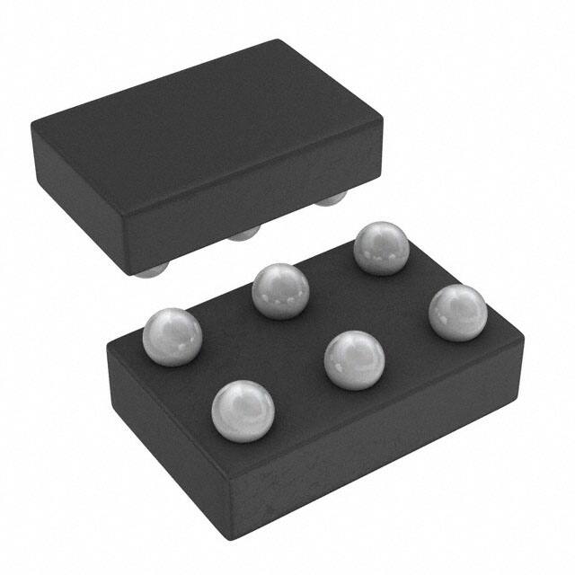
- Package: 8-pin, D-Type Flip-Flop
- Essence: High-performance, low-power consumption flip-flop
- Packaging/Quantity: Tape and Reel, 2500 units per reel
Specifications
- Supply Voltage Range: 1.65V to 5.5V
- Input Voltage Range: 0V to VCC
- Output Voltage Range: 0V to VCC
- Operating Temperature Range: -40°C to +85°C
- Propagation Delay Time: 4.3ns (typical)
- Output Drive Capability: ±24mA at 3.3V
- Power Dissipation: 2.5mW (typical)
Detailed Pin Configuration
The SN74LVC1G374YEPR has the following pin configuration:
```
| | --| CLR Q |-- --| D GND |-- --| CP VCC |-- --| OE /Q |-- --| D |-- --| Q |-- --| GND|-- |___________| ```
Functional Features
- Single positive-edge-triggered D-type flip-flop
- Clear (CLR) input for synchronous reset
- Clock (CP) input for triggering the flip-flop
- Data (D) input for storing the data
- Output Enable (OE) input for enabling/disabling the outputs
- Complementary outputs (Q and /Q) for storing the data
Advantages and Disadvantages
Advantages: - High-performance operation - Low-voltage operation - Low-power consumption - Small package size - Wide operating temperature range
Disadvantages: - Limited output drive capability - Single flip-flop functionality
Working Principles
The SN74LVC1G374YEPR is a single-gate D-type flip-flop that operates on a positive-edge-triggered clock signal. When the clock input (CP) transitions from low to high, the data input (D) is stored in the flip-flop and reflected at the outputs (Q and /Q). The clear input (CLR) can be used to reset the flip-flop synchronously. The output enable input (OE) allows for enabling or disabling the outputs.
Detailed Application Field Plans
The SN74LVC1G374YEPR is commonly used in various digital systems where a single flip-flop is required. Some of its application fields include:
- Microcontrollers: Used for storing and manipulating data in microcontroller circuits.
- Communication Systems: Employed in data transmission and reception circuits.
- Memory Modules: Integrated into memory modules for data storage and retrieval.
- Industrial Automation: Utilized in control systems for sequential logic operations.
- Consumer Electronics: Found in devices like smartphones, tablets, and gaming consoles.
Detailed and Complete Alternative Models
- SN74LVC1G175DBVR: Similar single-gate D-type flip-flop with different package and pin configuration.
- SN74LVC1G273DCKR: Octal D-type flip-flop with similar characteristics but multiple flip-flops in one package.
- SN74LVC1G80DBVR: Single-gate JK flip-flop with similar voltage range and package.
These alternative models provide similar functionality and can be considered as substitutes for the SN74LVC1G374YEPR in different applications.
Word count: 446 words
قم بإدراج 10 أسئلة وإجابات شائعة تتعلق بتطبيق SN74LVC1G374YEPR في الحلول التقنية
Sure! Here are 10 common questions and answers related to the application of SN74LVC1G374YEPR in technical solutions:
Q1: What is SN74LVC1G374YEPR? A1: SN74LVC1G374YEPR is a single D-type flip-flop with 3-state output, designed for low-voltage (1.65V to 5.5V) applications.
Q2: What is the purpose of SN74LVC1G374YEPR? A2: SN74LVC1G374YEPR is used to store and control digital data in various electronic circuits and systems.
Q3: What are the key features of SN74LVC1G374YEPR? A3: Some key features include high-speed operation, low power consumption, wide operating voltage range, and 3-state outputs.
Q4: What is the maximum operating frequency of SN74LVC1G374YEPR? A4: The maximum operating frequency of SN74LVC1G374YEPR is typically around 400 MHz.
Q5: How many flip-flops are there in SN74LVC1G374YEPR? A5: SN74LVC1G374YEPR consists of a single D-type flip-flop.
Q6: Can SN74LVC1G374YEPR be used in both input and output applications? A6: Yes, SN74LVC1G374YEPR can be used as both an input and output device depending on the circuit configuration.
Q7: What is the output drive capability of SN74LVC1G374YEPR? A7: SN74LVC1G374YEPR has a typical output drive capability of ±24 mA.
Q8: Is SN74LVC1G374YEPR compatible with other logic families? A8: Yes, SN74LVC1G374YEPR is compatible with a wide range of logic families due to its 3.3V and 5V tolerant inputs.
Q9: Can SN74LVC1G374YEPR be used in battery-powered applications? A9: Yes, SN74LVC1G374YEPR is suitable for battery-powered applications due to its low power consumption characteristics.
Q10: What are some typical applications of SN74LVC1G374YEPR? A10: Some typical applications include data storage, address latching, signal buffering, level shifting, and general-purpose digital logic circuits.
Please note that the answers provided here are general and may vary depending on specific circuit requirements and design considerations.