

SN74LVC1G99YEPR
Product Overview
- Category: Integrated Circuit (IC)
- Use: Logic Gate
- Characteristics: Single Gate, Low Voltage, CMOS Technology
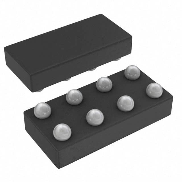
- Package: 6-Bump DSBGA (0.8mm x 0.8mm)
- Essence: NAND Gate with Schmitt Trigger Input
- Packaging/Quantity: Tape and Reel, 3000 units per reel
Specifications
- Supply Voltage Range: 1.65V to 5.5V
- High-Level Input Voltage: 0.7 x VCC
- Low-Level Input Voltage: 0.3 x VCC
- High-Level Output Voltage: 0.9 x VCC
- Low-Level Output Voltage: 0.1 x VCC
- Propagation Delay: 4.2ns (typical)
- Operating Temperature Range: -40°C to +85°C
Detailed Pin Configuration
The SN74LVC1G99YEPR has the following pin configuration:
____
   A --|    |-- VCC
   B --|    |-- Y
 GND --|____|-- NC
Functional Features
- NAND gate with Schmitt trigger input for noise immunity
- Wide supply voltage range allows compatibility with various systems
- Low power consumption due to CMOS technology
- Fast propagation delay for high-speed applications
- Small package size enables space-saving designs
Advantages
- Provides noise immunity through the Schmitt trigger input
- Versatile supply voltage range allows integration into different systems
- Low power consumption makes it suitable for battery-powered devices
- Fast propagation delay enables high-speed signal processing
- Compact package size facilitates miniaturization of electronic circuits
Disadvantages
- Limited number of gates in a single package
- Not suitable for high-power applications due to low voltage range
Working Principles
The SN74LVC1G99YEPR is a NAND gate with a Schmitt trigger input. It operates based on the principles of Complementary Metal-Oxide-Semiconductor (CMOS) technology. The Schmitt trigger input provides noise immunity by ensuring that the output transitions occur at different voltage levels for rising and falling input signals. This feature helps in reducing false triggering caused by noise or signal fluctuations.
Detailed Application Field Plans
The SN74LVC1G99YEPR can be used in various applications, including:
- Digital logic circuits
- Signal conditioning
- Level shifting
- Oscillators and timers
- Data transmission systems
- Battery-powered devices
- Industrial automation
- Automotive electronics
Detailed and Complete Alternative Models
Some alternative models that offer similar functionality to the SN74LVC1G99YEPR are:
- 74HC1G00: Single 2-Input NAND Gate
- 74HCT1G00: Single 2-Input NAND Gate with Schmitt Trigger Input
- CD4011B: Quad 2-Input NAND Gate
- MC74VHC1G00: Single 2-Input NAND Gate with Schmitt Trigger Input
- TC7SZ00F: Single 2-Input NAND Gate
These alternative models provide options with varying features, package sizes, and voltage ranges to suit different design requirements.
In conclusion, the SN74LVC1G99YEPR is a single NAND gate with a Schmitt trigger input. It offers noise immunity, low power consumption, and fast propagation delay. With its wide supply voltage range and compact package size, it finds applications in various digital logic circuits, signal conditioning, and level shifting tasks. Alternative models provide flexibility in terms of features and package options.
قم بإدراج 10 أسئلة وإجابات شائعة تتعلق بتطبيق SN74LVC1G99YEPR في الحلول التقنية
Sure! Here are 10 common questions and answers related to the application of SN74LVC1G99YEPR in technical solutions:
Q1: What is the SN74LVC1G99YEPR? A1: The SN74LVC1G99YEPR is a single-bit dual-supply bus switch with configurable voltage translation and integrated pull-up resistors.
Q2: What is the purpose of the SN74LVC1G99YEPR? A2: The purpose of this device is to provide bidirectional level shifting between different voltage domains in a circuit.
Q3: What voltage levels can the SN74LVC1G99YEPR support? A3: It can support voltage levels ranging from 1.65V to 5.5V.
Q4: How many channels does the SN74LVC1G99YEPR have? A4: This device has a single channel, allowing for one bidirectional signal connection.
Q5: Can the SN74LVC1G99YEPR handle high-speed signals? A5: Yes, it is designed to support high-speed data transmission up to 100 MHz.
Q6: Does the SN74LVC1G99YEPR have built-in pull-up resistors? A6: Yes, it has integrated pull-up resistors that can be enabled or disabled based on the application requirements.
Q7: Can the SN74LVC1G99YEPR be used in battery-powered applications? A7: Yes, it can be used in battery-powered applications as it supports low power consumption.
Q8: Is the SN74LVC1G99YEPR compatible with other logic families? A8: Yes, it is compatible with both CMOS and TTL logic families.
Q9: What is the package type of the SN74LVC1G99YEPR? A9: It is available in a small SOT-23 package, which is suitable for space-constrained designs.
Q10: Are there any application notes or reference designs available for the SN74LVC1G99YEPR? A10: Yes, Texas Instruments provides application notes and reference designs that can help with the implementation of this device in various technical solutions.
Please note that these answers are general and may vary depending on specific application requirements.