

SN74LVC2G34DRLR
Product Overview
Category
The SN74LVC2G34DRLR belongs to the category of integrated circuits (ICs).
Use
This IC is commonly used as a dual buffer/driver with open-drain outputs.
Characteristics
- Dual buffer/driver with open-drain outputs
- High-speed operation
- Low power consumption
- Wide operating voltage range
- Schmitt-trigger inputs for noise immunity
- Available in small package size
Package
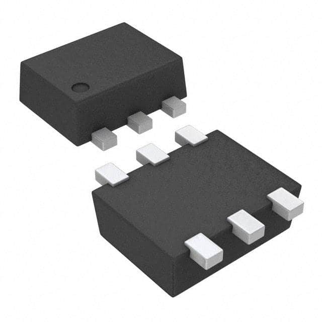
The SN74LVC2G34DRLR is available in a small package known as VSON-8, which stands for Very Small Outline No-Lead. This package offers a compact form factor and is suitable for space-constrained applications.
Essence
The essence of the SN74LVC2G34DRLR lies in its ability to provide buffering and driving capabilities with open-drain outputs, making it suitable for various digital signal applications.
Packaging/Quantity
The SN74LVC2G34DRLR is typically packaged in reels containing 3000 units per reel.
Specifications
- Supply Voltage Range: 1.65V to 5.5V
- Input Voltage Range: -0.5V to VCC + 0.5V
- Output Voltage Range: 0V to VCC
- Operating Temperature Range: -40°C to +85°C
- Maximum Propagation Delay: 3.9ns (typical)
- Maximum Quiescent Current: 10μA (typical)
Detailed Pin Configuration
The SN74LVC2G34DRLR has a total of 8 pins arranged as follows:
___________
      |           |
   1 -| A         |-
   2 -| B         |-
   3 -| Y         |-
   4 -| GND       |-
   5 -| Y         |-
   6 -| B         |-
   7 -| A         |-
   8 -| VCC       |-
      |___________|
Functional Features
- Dual buffer/driver: The SN74LVC2G34DRLR provides two independent buffer/driver circuits.
- Open-drain outputs: The outputs of this IC are open-drain, allowing for easy interfacing with other devices.
- High-speed operation: The IC operates at high speeds, making it suitable for time-critical applications.
- Low power consumption: The SN74LVC2G34DRLR is designed to consume minimal power, enhancing energy efficiency.
- Schmitt-trigger inputs: The IC features Schmitt-trigger inputs, providing noise immunity and reliable signal detection.
Advantages and Disadvantages
Advantages
- Compact package size enables space-saving designs.
- Wide operating voltage range allows compatibility with various systems.
- High-speed operation facilitates quick signal processing.
- Low power consumption contributes to energy-efficient applications.
- Schmitt-trigger inputs enhance noise immunity and signal integrity.
Disadvantages
- Limited number of buffer/driver circuits (two in total).
- Open-drain outputs may require additional pull-up resistors in certain applications.
Working Principles
The SN74LVC2G34DRLR functions as a buffer/driver with open-drain outputs. It receives input signals on pins A and B, and the corresponding buffered output signals are available on pins Y. The open-drain outputs allow for easy connection to other devices by providing flexibility in determining the logic levels.
Detailed Application Field Plans
The SN74LVC2G34DRLR finds applications in various fields, including but not limited to: 1. Digital communication systems 2. Industrial automation 3. Consumer electronics 4. Automotive electronics 5. Medical devices
Detailed and Complete Alternative Models
- SN74LVC2G34DCKR: Similar to SN74LVC2G34DRLR, but available in SC-70 package.
- SN74LVC2G34DBVR: Similar to SN74LVC2G34DRLR, but available in SOT-23 package.
- SN74LVC2G34DCUR: Similar to SN74LVC2G34DRLR, but available in US8 package.
These alternative models offer similar functionality with slight variations in package size and pin configuration.
In conclusion, the SN74LVC2G34DRLR is a dual buffer/driver IC with open-drain outputs. It offers high-speed operation, low power consumption, and wide operating voltage range. Its compact package size and Schmitt-trigger inputs make it suitable for various digital signal applications. However, it has a limited number of buffer/driver circuits and may require additional pull-up resistors in certain cases. The IC
قم بإدراج 10 أسئلة وإجابات شائعة تتعلق بتطبيق SN74LVC2G34DRLR في الحلول التقنية
Sure! Here are 10 common questions and answers related to the application of SN74LVC2G34DRLR in technical solutions:
Q: What is the SN74LVC2G34DRLR? A: The SN74LVC2G34DRLR is a dual buffer gate IC (integrated circuit) with open-drain outputs, commonly used for signal buffering and level shifting applications.
Q: What is the operating voltage range of SN74LVC2G34DRLR? A: The SN74LVC2G34DRLR operates within a voltage range of 1.65V to 5.5V.
Q: What is the maximum output current of SN74LVC2G34DRLR? A: The SN74LVC2G34DRLR can source or sink up to 32mA of current per output.
Q: Can I use SN74LVC2G34DRLR for level shifting between different voltage domains? A: Yes, the SN74LVC2G34DRLR can be used for level shifting between different voltage domains as long as the voltage levels are within its operating range.
Q: Does SN74LVC2G34DRLR have built-in protection features? A: Yes, the SN74LVC2G34DRLR has built-in ESD (electrostatic discharge) protection on its inputs and outputs.
Q: What is the propagation delay of SN74LVC2G34DRLR? A: The typical propagation delay of SN74LVC2G34DRLR is around 3.8ns.
Q: Can I connect multiple SN74LVC2G34DRLR devices in parallel to increase the output current? A: No, connecting multiple SN74LVC2G34DRLR devices in parallel is not recommended as it may cause issues with signal integrity and timing.
Q: Can I use SN74LVC2G34DRLR for bidirectional level shifting? A: No, the SN74LVC2G34DRLR is a unidirectional buffer gate and cannot be used for bidirectional level shifting.
Q: What is the package type of SN74LVC2G34DRLR? A: The SN74LVC2G34DRLR is available in a small SOT-553 package.
Q: Are there any application notes or reference designs available for SN74LVC2G34DRLR? A: Yes, Texas Instruments provides application notes and reference designs for SN74LVC2G34DRLR on their website, which can help you understand its usage in various technical solutions.
Please note that these answers are general and may vary depending on specific design requirements and datasheet specifications.