

SN74LVC2G74YEAR
Basic Information Overview
- Category: Integrated Circuit (IC)
- Use: Flip-Flop
- Characteristics: Low-voltage, dual positive-edge-triggered D-type flip-flop
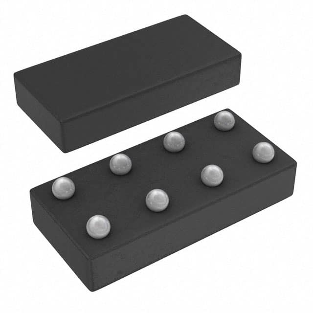
- Package: 8-pin small-outline integrated circuit (SOIC)
- Essence: Sequential logic device used for storing and transferring binary data
- Packaging/Quantity: Available in reels of 2500 units
Specifications
- Supply Voltage Range: 1.65V to 5.5V
- High-Level Input Voltage: 0.7 x VCC
- Low-Level Input Voltage: 0.3 x VCC
- High-Level Output Voltage: 0.9 x VCC
- Low-Level Output Voltage: 0.1 x VCC
- Maximum Operating Frequency: 100 MHz
- Propagation Delay Time: 4.6 ns (typical)
Detailed Pin Configuration
The SN74LVC2G74YEAR has the following pin configuration:
___________
      |           |
   1 -| CLR       |-
   2 -| D         |-
   3 -| CP        |-
   4 -| Q         |-
   5 -| GND       |-
   6 -| Q'        |-
   7 -| PRE       |-
   8 -| VCC       |-
      |___________|
Functional Features
- Dual positive-edge-triggered D-type flip-flops with clear and preset inputs
- Data is transferred to the outputs on the rising edge of the clock signal
- Clear input (CLR) sets both outputs to a low state
- Preset input (PRE) sets both outputs to a high state
- Can be used as a divide-by-two counter or frequency divider
Advantages and Disadvantages
Advantages: - Low-voltage operation allows for compatibility with a wide range of systems - Small package size enables space-saving designs - High-speed operation suitable for various applications
Disadvantages: - Limited number of flip-flops in a single package - May require additional components for complex sequential logic circuits
Working Principles
The SN74LVC2G74YEAR is a positive-edge-triggered D-type flip-flop. It stores and transfers binary data using two flip-flops. The clock input (CP) controls the transfer of data from the D input to the Q and Q' outputs. On the rising edge of the clock signal, the data at the D input is latched and appears at the outputs. The clear input (CLR) sets both outputs to a low state, while the preset input (PRE) sets both outputs to a high state.
Detailed Application Field Plans
The SN74LVC2G74YEAR can be used in various applications, including: 1. Digital communication systems 2. Microcontrollers and microprocessors 3. Data storage devices 4. Industrial automation 5. Automotive electronics
Detailed and Complete Alternative Models
Some alternative models to the SN74LVC2G74YEAR include: - CD4013B: Dual D-type flip-flop with similar characteristics - MC74HC74A: Dual positive-edge-triggered D-type flip-flop with clear and preset inputs - 74HCT74: Dual D-type flip-flop with set and reset inputs
These alternative models offer similar functionality and can be used as substitutes depending on specific requirements.
Word count: 314 words
قم بإدراج 10 أسئلة وإجابات شائعة تتعلق بتطبيق SN74LVC2G74YEAR في الحلول التقنية
Sure! Here are 10 common questions and answers related to the application of SN74LVC2G74YEAR in technical solutions:
Q: What is SN74LVC2G74YEAR? A: SN74LVC2G74YEAR is a dual positive-edge-triggered D-type flip-flop with clear, designed for 1.65-V to 5.5-V VCC operation.
Q: What are the key features of SN74LVC2G74YEAR? A: The key features include low power consumption, wide operating voltage range, high-speed operation, and compatibility with various logic families.
Q: What is the maximum operating frequency of SN74LVC2G74YEAR? A: The maximum operating frequency of SN74LVC2G74YEAR is typically around 100 MHz.
Q: Can SN74LVC2G74YEAR be used in battery-powered applications? A: Yes, SN74LVC2G74YEAR is suitable for battery-powered applications due to its low power consumption.
Q: How many flip-flops are there in SN74LVC2G74YEAR? A: SN74LVC2G74YEAR consists of two independent flip-flops.
Q: What is the purpose of the clear input in SN74LVC2G74YEAR? A: The clear input allows the user to reset the flip-flop to a known state.
Q: Can SN74LVC2G74YEAR operate at different supply voltages? A: Yes, SN74LVC2G74YEAR can operate within a wide supply voltage range of 1.65V to 5.5V.
Q: Is SN74LVC2G74YEAR compatible with other logic families? A: Yes, SN74LVC2G74YEAR is compatible with both TTL and CMOS logic families.
Q: What is the typical propagation delay of SN74LVC2G74YEAR? A: The typical propagation delay of SN74LVC2G74YEAR is around 3.5 ns.
Q: Can SN74LVC2G74YEAR be used in high-speed applications? A: Yes, SN74LVC2G74YEAR is designed for high-speed operation and can be used in various high-speed applications.
Please note that these answers are general and may vary depending on specific application requirements.