

SN74LVC2G74YZAR
Product Overview
- Category: Integrated Circuit (IC)
- Use: Flip-Flop
- Characteristics: Low-voltage, dual positive-edge-triggered D-type flip-flop
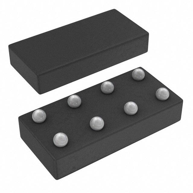
- Package: 8-pin small-outline integrated circuit (SOIC)
- Essence: This IC is designed to store and transfer data in electronic circuits.
- Packaging/Quantity: Available in tape and reel packaging with a quantity of 2500 units per reel.
Specifications
- Supply Voltage Range: 1.65V to 5.5V
- High-Level Input Voltage: 0.7 x Vcc
- Low-Level Input Voltage: 0.3 x Vcc
- High-Level Output Voltage: 0.9 x Vcc
- Low-Level Output Voltage: 0.1 x Vcc
- Maximum Operating Frequency: 100 MHz
- Propagation Delay Time: 4.6 ns
- Operating Temperature Range: -40°C to +85°C
Detailed Pin Configuration
The SN74LVC2G74YZAR has the following pin configuration:
___________
      |           |
   1 -| CLR       |-
   2 -| D         |-
   3 -| CP        |-
   4 -| Q         |-
   5 -| Q̅        |-
   6 -| GND       |-
   7 -| VCC       |-
      |___________|
Functional Features
- Dual positive-edge-triggered D-type flip-flop with clear (CLR) input
- Data (D) input for each flip-flop
- Clock (CP) input for controlling the flip-flop operation
- Outputs (Q and Q̅) provide the stored data
- Clear (CLR) input resets the flip-flop to a known state
Advantages and Disadvantages
Advantages: - Low-voltage operation allows for compatibility with various electronic systems - Small package size enables space-saving designs - High operating frequency allows for fast data transfer - Clear input provides a convenient way to reset the flip-flop
Disadvantages: - Limited number of flip-flops in a single IC package - Not suitable for high-power applications due to low voltage operation
Working Principles
The SN74LVC2G74YZAR operates based on positive-edge-triggered D-type flip-flop logic. The flip-flop stores and transfers data based on the clock signal (CP) and data input (D). When the clock signal transitions from low to high, the data at the D input is captured and stored in the flip-flop. The stored data is then available at the outputs (Q and Q̅). The clear input (CLR) can be used to reset the flip-flop to a known state.
Detailed Application Field Plans
The SN74LVC2G74YZAR is commonly used in various digital systems and applications, including but not limited to: - Microcontrollers - Data storage devices - Communication systems - Consumer electronics - Industrial automation
Detailed and Complete Alternative Models
Some alternative models that serve similar functions to the SN74LVC2G74YZAR include: - MC74VHC1G74: Single positive-edge-triggered D-type flip-flop - CD4013B: Dual D-type flip-flop with set and reset inputs - 74HC74: Dual D-type flip-flop with clear input
These alternative models offer different specifications and features, allowing designers to choose the most suitable option for their specific application requirements.
Word count: 389 words
قم بإدراج 10 أسئلة وإجابات شائعة تتعلق بتطبيق SN74LVC2G74YZAR في الحلول التقنية
Sure! Here are 10 common questions and answers related to the application of SN74LVC2G74YZAR in technical solutions:
Q: What is SN74LVC2G74YZAR? A: SN74LVC2G74YZAR is a dual positive-edge-triggered D-type flip-flop integrated circuit (IC) manufactured by Texas Instruments.
Q: What is the operating voltage range for SN74LVC2G74YZAR? A: The operating voltage range for SN74LVC2G74YZAR is typically between 1.65V and 5.5V.
Q: What is the maximum clock frequency supported by SN74LVC2G74YZAR? A: SN74LVC2G74YZAR can support clock frequencies up to 100 MHz.
Q: Can SN74LVC2G74YZAR be used as a level shifter? A: Yes, SN74LVC2G74YZAR can be used as a level shifter to convert signals between different voltage levels.
Q: How many flip-flops are present in SN74LVC2G74YZAR? A: SN74LVC2G74YZAR contains two independent D-type flip-flops.
Q: What is the typical propagation delay of SN74LVC2G74YZAR? A: The typical propagation delay of SN74LVC2G74YZAR is around 4.7 ns.
Q: Is SN74LVC2G74YZAR suitable for high-speed applications? A: Yes, SN74LVC2G74YZAR is designed for high-speed operation and can be used in various high-frequency applications.
Q: Can SN74LVC2G74YZAR be used in battery-powered devices? A: Yes, SN74LVC2G74YZAR has a low power consumption and can be used in battery-powered devices.
Q: What is the package type of SN74LVC2G74YZAR? A: SN74LVC2G74YZAR is available in a small-outline transistor (SOT) package.
Q: Are there any recommended applications for SN74LVC2G74YZAR? A: SN74LVC2G74YZAR is commonly used in applications such as data storage, clock synchronization, and general-purpose digital logic circuits.
Please note that these answers are general and may vary depending on specific design requirements and application scenarios.