

SN74LVC3G07YZPR
Product Overview
Category
The SN74LVC3G07YZPR belongs to the category of integrated circuits (ICs).
Use
This IC is commonly used as a buffer or driver in various electronic devices and systems.
Characteristics
- Low-voltage CMOS technology
- High-speed operation
- Wide operating voltage range
- Low power consumption
- Small package size
Package
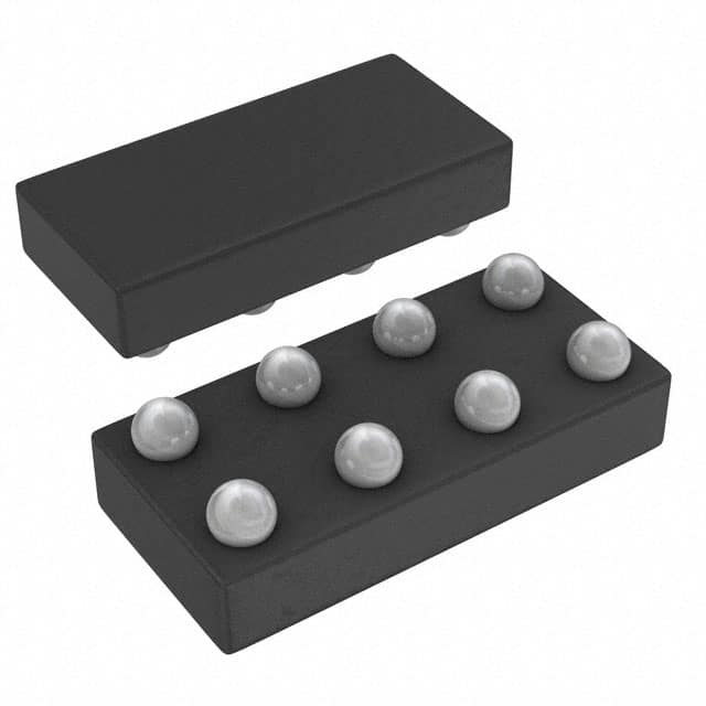
The SN74LVC3G07YZPR is available in a small-outline transistor (SOT) package.
Essence
The essence of this product lies in its ability to provide buffering and driving capabilities for digital signals in low-voltage applications.
Packaging/Quantity
The SN74LVC3G07YZPR is typically packaged in reels, with each reel containing a specific quantity of ICs. The exact quantity may vary depending on the manufacturer's specifications.
Specifications
- Supply Voltage: 1.65V to 5.5V
- Input Voltage Range: GND to VCC
- Output Voltage Range: GND to VCC
- Operating Temperature Range: -40°C to +85°C
- Maximum Propagation Delay: 4.3 ns
- Maximum Output Current: ±32 mA
Detailed Pin Configuration
The SN74LVC3G07YZPR has a total of six pins, which are labeled as follows:
- A Input
- Y Output
- B Input
- C Input
- GND (Ground)
- VCC (Power Supply)
Functional Features
- Buffering: The SN74LVC3G07YZPR can amplify weak input signals to ensure proper signal integrity.
- Driving: It can drive signals with sufficient current to interface with other components or systems.
- Logic Level Shifting: This IC can convert logic levels between different voltage domains.
- Noise Filtering: It helps in reducing noise and improving signal quality.
Advantages and Disadvantages
Advantages
- Low power consumption makes it suitable for battery-powered devices.
- Wide operating voltage range allows compatibility with various systems.
- High-speed operation enables efficient signal processing.
- Small package size saves board space in compact designs.
Disadvantages
- Limited output current may restrict its use in high-power applications.
- Propagation delay may affect real-time applications with strict timing requirements.
Working Principles
The SN74LVC3G07YZPR operates based on complementary metal-oxide-semiconductor (CMOS) technology. It utilizes a combination of transistors to amplify and drive digital signals. The input signals are buffered and amplified, while the output stage provides sufficient current to drive external loads.
Detailed Application Field Plans
The SN74LVC3G07YZPR finds applications in various fields, including:
- Consumer Electronics: Used in smartphones, tablets, and portable media players for signal buffering and level shifting.
- Automotive: Employed in automotive electronics for driving sensors, actuators, and communication interfaces.
- Industrial Automation: Utilized in control systems, PLCs, and motor drives for signal amplification and interfacing.
- Communication Systems: Integrated into networking equipment, routers, and switches for signal conditioning and level conversion.
Detailed and Complete Alternative Models
- SN74LVC3G17: Similar functionality with Schmitt-trigger inputs for improved noise immunity.
- SN74LVC3G34: Provides three buffers with open-drain outputs for wired-OR applications.
- SN74LVC3G04: Inverter gate IC with similar characteristics but different pin configuration.
These alternative models offer similar features and can be used as substitutes depending on specific application requirements.
Word count: 511
قم بإدراج 10 أسئلة وإجابات شائعة تتعلق بتطبيق SN74LVC3G07YZPR في الحلول التقنية
Sure! Here are 10 common questions and answers related to the application of SN74LVC3G07YZPR in technical solutions:
Q: What is SN74LVC3G07YZPR? A: SN74LVC3G07YZPR is a triple buffer/driver with open-drain outputs, commonly used in digital logic applications.
Q: What is the voltage range supported by SN74LVC3G07YZPR? A: SN74LVC3G07YZPR supports a voltage range from 1.65V to 5.5V.
Q: What is the maximum output current of SN74LVC3G07YZPR? A: The maximum output current of SN74LVC3G07YZPR is typically 32mA.
Q: Can SN74LVC3G07YZPR be used for level shifting between different voltage domains? A: Yes, SN74LVC3G07YZPR can be used for level shifting between different voltage domains due to its wide voltage range support.
Q: How many buffers/drivers are there in SN74LVC3G07YZPR? A: SN74LVC3G07YZPR consists of three independent buffers/drivers.
Q: What is the purpose of the open-drain outputs in SN74LVC3G07YZPR? A: The open-drain outputs allow for wired-OR connections and provide flexibility in designing multi-voltage systems.
Q: Can SN74LVC3G07YZPR handle high-speed signals? A: Yes, SN74LVC3G07YZPR is designed to handle high-speed signals with a typical propagation delay of 3.8ns.
Q: Is SN74LVC3G07YZPR suitable for battery-powered applications? A: Yes, SN74LVC3G07YZPR is suitable for battery-powered applications as it operates at low power and supports a wide voltage range.
Q: Can SN74LVC3G07YZPR be used in both input and output applications? A: Yes, SN74LVC3G07YZPR can be used as both an input buffer and an output driver depending on the application requirements.
Q: Are there any special considerations when using SN74LVC3G07YZPR in high-noise environments? A: It is recommended to use proper decoupling capacitors near the power supply pins of SN74LVC3G07YZPR to minimize noise interference.
Please note that these answers are general and may vary based on specific application requirements.