

SN74LVC574ADGVRE4
Product Overview
Category
The SN74LVC574ADGVRE4 belongs to the category of integrated circuits (ICs).
Use
This IC is commonly used for data storage and transfer in digital systems.
Characteristics
- Low-voltage CMOS technology
- High-speed operation
- Wide operating voltage range
- Schmitt-trigger inputs for noise immunity
- 3-state outputs for bus-oriented applications
Package
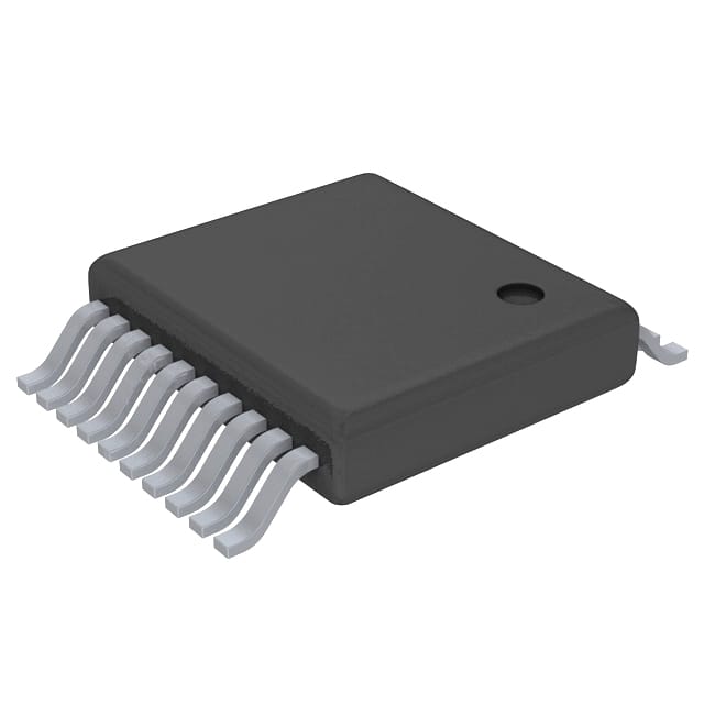
The SN74LVC574ADGVRE4 is available in a small package with a VQFN-20 footprint.
Essence
The essence of this product lies in its ability to store and transfer digital data efficiently and reliably.
Packaging/Quantity
The SN74LVC574ADGVRE4 is typically packaged in reels, with each reel containing a specific quantity of ICs. The exact quantity may vary depending on the manufacturer's specifications.
Specifications
- Supply Voltage: 1.65V to 5.5V
- Input Voltage Range: 0V to VCC
- Output Voltage Range: 0V to VCC
- Operating Temperature Range: -40°C to +85°C
- Maximum Clock Frequency: 100MHz
- Number of Flip-Flops: 8
Detailed Pin Configuration
The SN74LVC574ADGVRE4 has a total of 20 pins. The pin configuration is as follows:
- GND (Ground)
- D0 (Data Input 0)
- D1 (Data Input 1)
- D2 (Data Input 2)
- D3 (Data Input 3)
- D4 (Data Input 4)
- D5 (Data Input 5)
- D6 (Data Input 6)
- D7 (Data Input 7)
- OE (Output Enable)
- CP (Clock Pulse)
- MR (Master Reset)
- Q0 (Flip-Flop Output 0)
- Q1 (Flip-Flop Output 1)
- Q2 (Flip-Flop Output 2)
- Q3 (Flip-Flop Output 3)
- Q4 (Flip-Flop Output 4)
- Q5 (Flip-Flop Output 5)
- Q6 (Flip-Flop Output 6)
- VCC (Supply Voltage)
Functional Features
- Data storage and transfer: The SN74LVC574ADGVRE4 has 8 flip-flops that can store digital data. It allows for efficient transfer of data between different parts of a digital system.
- Output enable control: The OE pin enables or disables the outputs, making it suitable for bus-oriented applications.
- Schmitt-trigger inputs: These inputs provide noise immunity, ensuring reliable operation even in noisy environments.
- Wide operating voltage range: The IC can operate within a wide voltage range, making it compatible with various power supply configurations.
Advantages and Disadvantages
Advantages
- High-speed operation allows for quick data transfer.
- Low-voltage CMOS technology reduces power consumption.
- Schmitt-trigger inputs provide noise immunity, enhancing reliability.
- 3-state outputs enable bus-oriented applications.
Disadvantages
- Limited number of flip-flops (8) may not be sufficient for certain applications requiring more storage capacity.
- Availability and pricing may vary depending on the manufacturer and market conditions.
Working Principles
The SN74LVC574ADGVRE4 operates based on the principles of digital logic. It utilizes flip-flops to store and transfer binary data. The clock pulse (CP) controls the timing of data transfer, while the master reset (MR) allows for resetting the flip-flops to a known state. The output enable (OE) pin enables or disables the outputs, allowing for bus-oriented applications.
Detailed Application Field Plans
The SN74LVC574ADGVRE4 finds applications in various digital systems, including but not limited to: - Microcontrollers - Data communication systems - Memory modules - Industrial automation - Automotive electronics
Detailed and Complete Alternative Models
Some alternative models that offer similar functionality to the SN74LVC574ADGVRE4 include: - 74HC574: This IC operates at higher voltages but provides similar data storage and transfer capabilities. - CD4013: A dual D-type flip-flop IC that can be used as an alternative for specific applications requiring fewer flip-flops. - SN74LVCH16245A: This IC is a bidirectional transceiver with 16-bit flip-flops, suitable for bus-oriented applications.
Please note that the availability and specifications of alternative models may vary. It is recommended to consult the manufacturer's datasheets for detailed information.
[Word Count: 536]
قم بإدراج 10 أسئلة وإجابات شائعة تتعلق بتطبيق SN74LVC574ADGVRE4 في الحلول التقنية
Sure! Here are 10 common questions and answers related to the application of SN74LVC574ADGVRE4:
Q: What is SN74LVC574ADGVRE4? A: SN74LVC574ADGVRE4 is a octal D-type flip-flop with 3-state outputs, designed for low-voltage (2.5V to 3.6V) applications.
Q: What is the maximum operating frequency of SN74LVC574ADGVRE4? A: The maximum operating frequency of SN74LVC574ADGVRE4 is typically around 100 MHz.
Q: What is the input voltage range for SN74LVC574ADGVRE4? A: The input voltage range for SN74LVC574ADGVRE4 is from ground to VCC.
Q: Can SN74LVC574ADGVRE4 be used in both digital and analog applications? A: No, SN74LVC574ADGVRE4 is specifically designed for digital applications and should not be used in analog circuits.
Q: What is the output current capability of SN74LVC574ADGVRE4? A: SN74LVC574ADGVRE4 has a typical output current capability of ±24 mA.
Q: Does SN74LVC574ADGVRE4 have internal pull-up or pull-down resistors? A: No, SN74LVC574ADGVRE4 does not have internal pull-up or pull-down resistors.
Q: Can SN74LVC574ADGVRE4 tolerate overvoltage on its inputs? A: Yes, SN74LVC574ADGVRE4 has protection diodes that can tolerate voltages up to VCC + 0.5V on its inputs.
Q: What is the power supply voltage range for SN74LVC574ADGVRE4? A: The power supply voltage range for SN74LVC574ADGVRE4 is from 2.5V to 3.6V.
Q: Can SN74LVC574ADGVRE4 be used in high-temperature environments? A: Yes, SN74LVC574ADGVRE4 has a specified operating temperature range of -40°C to 125°C.
Q: Is SN74LVC574ADGVRE4 available in different package options? A: Yes, SN74LVC574ADGVRE4 is available in various package options, such as TSSOP and TVSOP.
Please note that these answers are general and may vary depending on the specific datasheet and manufacturer's specifications.