

SN74LVC863ADBR
Product Overview
- Category: Integrated Circuit
- Use: Logic Gate
- Characteristics: Low Voltage, CMOS Technology
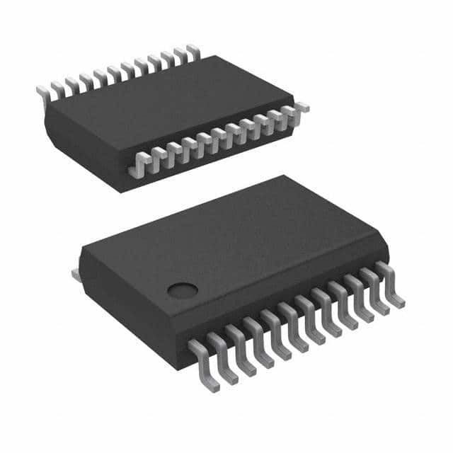
- Package: SSOP (Shrink Small Outline Package)
- Essence: High-Speed, Low-Power Buffer/Driver
- Packaging/Quantity: Tape and Reel, 2500 pieces per reel
Specifications
- Supply Voltage Range: 1.65V to 3.6V
- Input Voltage Range: 0V to VCC
- Output Voltage Range: 0V to VCC
- Operating Temperature Range: -40°C to +85°C
- Propagation Delay Time: 2.5ns (typical)
- Output Drive Capability: ±24mA
- ESD Protection: Human Body Model > 2000V
Detailed Pin Configuration
The SN74LVC863ADBR has a total of 20 pins arranged as follows:
- A1 - Input A1
- B1 - Input B1
- Y1 - Output Y1
- GND - Ground
- A2 - Input A2
- B2 - Input B2
- Y2 - Output Y2
- GND - Ground
- VCC - Power Supply
- OE - Output Enable
- A3 - Input A3
- B3 - Input B3
- Y3 - Output Y3
- GND - Ground
- A4 - Input A4
- B4 - Input B4
- Y4 - Output Y4
- GND - Ground
- NC - No Connection
- VCC - Power Supply
Functional Features
- High-Speed Operation: The SN74LVC863ADBR is designed for high-speed logic applications, providing fast propagation delay times.
- Low-Power Consumption: This integrated circuit utilizes CMOS technology, resulting in low power consumption and extended battery life.
- Output Drive Capability: The buffer/driver has a high output drive capability of ±24mA, allowing it to drive various loads.
- ESD Protection: The device offers robust electrostatic discharge (ESD) protection, ensuring its reliability in harsh environments.
Advantages and Disadvantages
Advantages: - High-speed operation enables efficient data processing. - Low-power consumption extends battery life in portable devices. - Robust ESD protection ensures reliability in challenging conditions.
Disadvantages: - Limited supply voltage range restricts compatibility with certain systems. - Package size may not be suitable for space-constrained applications.
Working Principles
The SN74LVC863ADBR is a buffer/driver that operates on a low voltage supply. It receives input signals from the A1-B4 pins and provides corresponding output signals on the Y1-Y4 pins. The OE pin controls the output enable function, allowing the user to enable or disable the outputs as needed. The device utilizes CMOS technology, which ensures low power consumption and high-speed operation.
Detailed Application Field Plans
The SN74LVC863ADBR can be used in various applications, including but not limited to: - Data communication systems - Computer peripherals - Industrial control systems - Automotive electronics - Consumer electronics
Detailed and Complete Alternative Models
Some alternative models that offer similar functionality to the SN74LVC863ADBR are: - SN74LVC861A - SN74LVC862A - SN74LVC864A - SN74LVC865A
These alternatives provide comparable features and can be considered based on specific application requirements.
Word count: 346 words
قم بإدراج 10 أسئلة وإجابات شائعة تتعلق بتطبيق SN74LVC863ADBR في الحلول التقنية
Sure! Here are 10 common questions and answers related to the application of SN74LVC863ADBR in technical solutions:
Q: What is the SN74LVC863ADBR? A: The SN74LVC863ADBR is a high-performance, low-voltage CMOS 9-bit universal shift register with 3-state outputs.
Q: What is the operating voltage range for SN74LVC863ADBR? A: The operating voltage range for SN74LVC863ADBR is 1.65V to 3.6V.
Q: What are the typical applications of SN74LVC863ADBR? A: SN74LVC863ADBR can be used in various applications such as data storage, serial-to-parallel conversion, parallel-to-serial conversion, and general-purpose shifting of data.
Q: What is the maximum clock frequency supported by SN74LVC863ADBR? A: The maximum clock frequency supported by SN74LVC863ADBR is typically 100 MHz.
Q: How many 3-state outputs does SN74LVC863ADBR have? A: SN74LVC863ADBR has nine 3-state outputs.
Q: Can SN74LVC863ADBR be cascaded to increase the number of bits? A: Yes, SN74LVC863ADBR can be cascaded to increase the number of bits by connecting the serial output of one device to the serial input of another.
Q: What is the power supply current consumption of SN74LVC863ADBR? A: The power supply current consumption of SN74LVC863ADBR is typically 8 mA.
Q: Does SN74LVC863ADBR have built-in protection features? A: Yes, SN74LVC863ADBR has built-in ESD protection and can withstand up to 2 kV of human-body model (HBM) electrostatic discharge.
Q: What is the package type for SN74LVC863ADBR? A: SN74LVC863ADBR is available in a TSSOP-48 package.
Q: Are there any recommended external components for using SN74LVC863ADBR? A: It is recommended to use bypass capacitors near the power supply pins to improve noise immunity and stability during operation.
Please note that these answers are general and may vary depending on the specific application and requirements.