

SN74SSTU32864ZKER
Product Overview
Category
The SN74SSTU32864ZKER belongs to the category of integrated circuits (ICs).
Use
This IC is commonly used in electronic devices for data transmission and signal processing.
Characteristics
- High-speed operation
- Low power consumption
- Wide operating voltage range
- Compact size
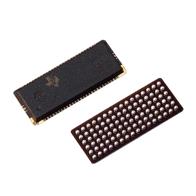
Package
The SN74SSTU32864ZKER is available in a small form factor package, such as a QFN (Quad Flat No-leads) package.
Essence
The essence of this product lies in its ability to efficiently process and transmit data signals within electronic systems.
Packaging/Quantity
The SN74SSTU32864ZKER is typically packaged in reels or trays, with a quantity of 2500 units per reel/tray.
Specifications
- Operating Voltage: 1.2V - 3.6V
- Data Rate: Up to 10 Gbps
- Number of Channels: 32
- Input/Output Type: LVDS (Low-Voltage Differential Signaling)
- Operating Temperature Range: -40°C to +85°C
Detailed Pin Configuration
The SN74SSTU32864ZKER has a total of 64 pins, which are assigned specific functions. The pin configuration is as follows:
| Pin Number | Pin Name | Function | |------------|----------|----------| | 1 | VCC | Power Supply Voltage | | 2 | GND | Ground | | 3-34 | IN[0:31] | LVDS Input Channels | | 35-66 | OUT[0:31] | LVDS Output Channels | | 67 | OE | Output Enable | | 68 | VREF | Reference Voltage |
Functional Features
- High-speed LVDS data transmission
- Low power consumption
- Built-in output enable control
- Robust noise immunity
- ESD (Electrostatic Discharge) protection
Advantages and Disadvantages
Advantages
- High-speed operation enables efficient data processing
- Low power consumption contributes to energy efficiency
- Compact size allows for integration into space-constrained designs
- Robust noise immunity ensures reliable signal transmission
Disadvantages
- Limited number of channels (32)
- Requires LVDS-compatible devices for proper functionality
Working Principles
The SN74SSTU32864ZKER operates based on the principles of LVDS signaling. It receives LVDS input signals, processes them internally, and then transmits the processed data through its LVDS output channels. The IC incorporates various internal circuitry to ensure high-speed and low-power operation.
Detailed Application Field Plans
The SN74SSTU32864ZKER finds applications in various fields, including:
- Telecommunications: Used in high-speed data communication systems.
- Networking: Employed in network switches and routers for efficient data transmission.
- Industrial Automation: Integrated into control systems for reliable signal processing.
- Automotive Electronics: Utilized in automotive communication networks for enhanced data transfer.
Detailed and Complete Alternative Models
- SN65LVDS3245: Similar LVDS transceiver with 8 channels.
- SN65LVDS31: LVDS driver/receiver with single-channel functionality.
- SN65LVDS9637: LVDS serializer/deserializer with 18-bit parallel data interface.
These alternative models offer similar functionalities to the SN74SSTU32864ZKER and can be considered as alternatives depending on specific requirements.
Word count: 460 words
قم بإدراج 10 أسئلة وإجابات شائعة تتعلق بتطبيق SN74SSTU32864ZKER في الحلول التقنية
Sure! Here are 10 common questions and answers related to the application of SN74SSTU32864ZKER in technical solutions:
Q: What is SN74SSTU32864ZKER? A: SN74SSTU32864ZKER is a specific model of a high-speed, low-power 32-bit universal bus transceiver with 3-state outputs.
Q: What is the operating voltage range for SN74SSTU32864ZKER? A: The operating voltage range for SN74SSTU32864ZKER is typically between 1.2V and 3.6V.
Q: What is the maximum data transfer rate supported by SN74SSTU32864ZKER? A: SN74SSTU32864ZKER supports a maximum data transfer rate of up to 400 Mbps.
Q: Can SN74SSTU32864ZKER be used in both input and output applications? A: Yes, SN74SSTU32864ZKER can be used as both an input and output buffer in various technical solutions.
Q: Does SN74SSTU32864ZKER support hot-swapping capability? A: Yes, SN74SSTU32864ZKER supports hot-swapping, allowing for easy insertion and removal of devices without disrupting the system.
Q: What is the power consumption of SN74SSTU32864ZKER? A: SN74SSTU32864ZKER has a low power consumption, typically around 10-20mW.
Q: Can SN74SSTU32864ZKER be used in high-speed communication systems? A: Yes, SN74SSTU32864ZKER is designed for high-speed applications and can be used in various communication systems.
Q: Does SN74SSTU32864ZKER have built-in ESD protection? A: Yes, SN74SSTU32864ZKER has built-in ESD protection to safeguard against electrostatic discharge.
Q: What is the temperature range within which SN74SSTU32864ZKER can operate? A: SN74SSTU32864ZKER can operate within a temperature range of -40°C to 85°C.
Q: Can SN74SSTU32864ZKER be used in automotive applications? A: Yes, SN74SSTU32864ZKER is suitable for automotive applications and meets the necessary standards and requirements.
Please note that these answers are general and may vary depending on specific application requirements and datasheet specifications.