

TLC7524IFNG3
Product Overview
Category
TLC7524IFNG3 belongs to the category of integrated circuits (ICs).
Use
This product is commonly used in electronic devices for digital-to-analog conversion.
Characteristics
- High precision and accuracy
- Low power consumption
- Wide operating voltage range
- Small package size
- Excellent linearity
Package
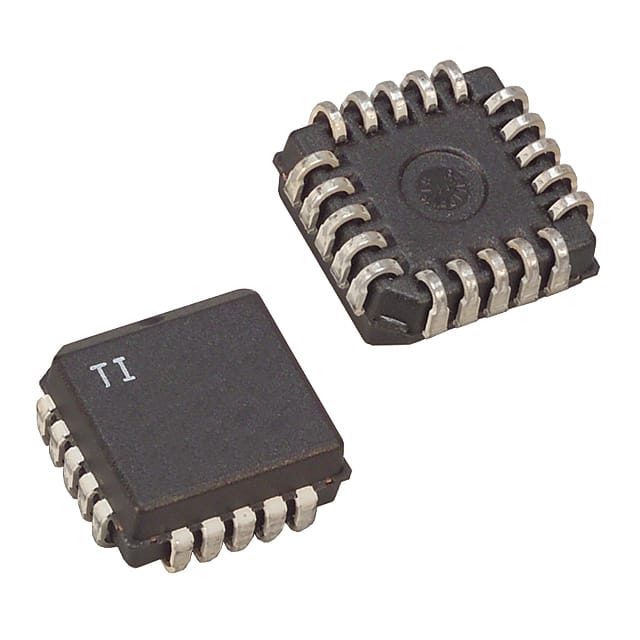
TLC7524IFNG3 is available in a small outline integrated circuit (SOIC) package.
Essence
The essence of TLC7524IFNG3 lies in its ability to convert digital signals into analog voltages with high precision and accuracy.
Packaging/Quantity
This product is typically packaged in reels or tubes, with a quantity of 250 units per reel/tube.
Specifications
- Resolution: 8 bits
- Number of channels: 4
- Supply voltage range: 2.7V to 5.5V
- Operating temperature range: -40°C to +85°C
- Output voltage range: 0V to Vref
Detailed Pin Configuration
- VDD: Positive supply voltage
- VREF: Reference voltage input
- AGND: Analog ground
- OUTA: Analog output channel A
- OUTB: Analog output channel B
- OUTC: Analog output channel C
- OUTD: Analog output channel D
- DGND: Digital ground
- CS: Chip select input
- CLK: Clock input
- DIN: Serial data input
- LDAC: Load DAC input
- REFOUT: Reference voltage output
- VSS: Negative supply voltage
Functional Features
- Serial interface for easy integration with microcontrollers
- Internal reference voltage generator
- Power-on reset circuitry
- Double-buffered input latch for simultaneous update of all channels
- Low glitch energy
Advantages and Disadvantages
Advantages
- High precision and accuracy in digital-to-analog conversion
- Low power consumption, suitable for battery-powered devices
- Wide operating voltage range allows for versatile applications
- Small package size saves board space
- Excellent linearity ensures faithful analog output representation
Disadvantages
- Limited resolution (8 bits) compared to higher-end DACs
- Not suitable for applications requiring ultra-high precision
Working Principles
TLC7524IFNG3 utilizes a combination of digital logic and resistor networks to convert digital signals into corresponding analog voltages. The digital input is processed internally and converted into an analog output voltage based on the reference voltage provided.
Detailed Application Field Plans
TLC7524IFNG3 finds application in various fields, including: 1. Industrial automation: Control systems, process monitoring, and data acquisition. 2. Audio equipment: Digital audio players, mixers, and amplifiers. 3. Instrumentation: Test and measurement equipment, signal generators, and oscilloscopes. 4. Communication systems: Modems, routers, and telecommunication devices. 5. Automotive electronics: Dashboard displays, climate control systems, and motor control.
Detailed and Complete Alternative Models
- MCP4921: 12-bit resolution, single-channel DAC with SPI interface.
- MAX5216: 16-bit resolution, quad-channel DAC with I2C interface.
- AD5620: 12-bit resolution, dual-channel DAC with serial interface.
These alternative models offer different resolutions, channel configurations, and communication interfaces to suit specific application requirements.
Word count: 408 words
قم بإدراج 10 أسئلة وإجابات شائعة تتعلق بتطبيق TLC7524IFNG3 في الحلول التقنية
Sure! Here are 10 common questions and answers related to the application of TLC7524IFNG3 in technical solutions:
Q: What is the TLC7524IFNG3? A: The TLC7524IFNG3 is a 12-bit digital-to-analog converter (DAC) integrated circuit.
Q: What is the operating voltage range of the TLC7524IFNG3? A: The TLC7524IFNG3 operates within a voltage range of 4.5V to 36V.
Q: How many channels does the TLC7524IFNG3 have? A: The TLC7524IFNG3 has 4 independent DAC channels.
Q: What is the resolution of the TLC7524IFNG3? A: The TLC7524IFNG3 has a resolution of 12 bits, allowing for 4096 possible output levels.
Q: Can the TLC7524IFNG3 be used in both single-ended and differential mode? A: Yes, the TLC7524IFNG3 can be used in both single-ended and differential mode, depending on the application requirements.
Q: What is the typical settling time of the TLC7524IFNG3? A: The typical settling time of the TLC7524IFNG3 is 10µs.
Q: Does the TLC7524IFNG3 require an external reference voltage? A: Yes, the TLC7524IFNG3 requires an external reference voltage for accurate conversion.
Q: What is the power supply rejection ratio (PSRR) of the TLC7524IFNG3? A: The PSRR of the TLC7524IFNG3 is typically 80dB.
Q: Can the TLC7524IFNG3 be used in industrial applications? A: Yes, the TLC7524IFNG3 is suitable for use in industrial applications due to its wide operating voltage range and robust design.
Q: What is the package type of the TLC7524IFNG3? A: The TLC7524IFNG3 is available in an 8-pin SOIC (Small Outline Integrated Circuit) package.
Please note that these answers are general and may vary depending on specific application requirements and datasheet specifications.