

TPS22913BYZVT
Product Overview
Category
The TPS22913BYZVT belongs to the category of power management integrated circuits (PMICs).
Use
It is primarily used for power distribution and control in various electronic devices.
Characteristics
- Low on-resistance
- Fast switching speed
- Wide input voltage range
- Overcurrent protection
- Thermal shutdown protection
Package
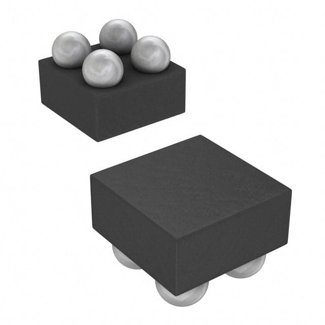
The TPS22913BYZVT is available in a small, surface-mount package.
Essence
The essence of TPS22913BYZVT lies in its ability to efficiently regulate and distribute power within electronic devices.
Packaging/Quantity
The product is typically packaged in reels or tubes, with a quantity of 2500 units per reel/tube.
Specifications
- Input Voltage Range: 2.5V to 5.5V
- On-Resistance: 30mΩ (typical)
- Maximum Continuous Current: 2A
- Operating Temperature Range: -40°C to +85°C
Detailed Pin Configuration
The TPS22913BYZVT has the following pin configuration:
- VIN: Input voltage pin
- EN: Enable pin
- GND: Ground pin
- VOUT: Output voltage pin
Functional Features
- Power sequencing capability
- Undervoltage lockout
- Reverse current blocking
- Low quiescent current
- Adjustable overcurrent limit
Advantages and Disadvantages
Advantages
- Efficient power distribution
- Fast switching speed
- Wide input voltage range
- Overcurrent and thermal protection
Disadvantages
- Limited maximum continuous current capacity
- Relatively high on-resistance
Working Principles
The TPS22913BYZVT operates by controlling the flow of power from the input voltage (VIN) to the output voltage (VOUT) based on the enable signal (EN). It utilizes a low on-resistance MOSFET to minimize power losses and ensure efficient power distribution.
Detailed Application Field Plans
The TPS22913BYZVT finds applications in various electronic devices, including but not limited to: - Mobile phones - Tablets - Portable gaming consoles - Wearable devices - IoT devices
Detailed and Complete Alternative Models
- TPS22914BYZVT
- TPS22915BYZVT
- TPS22916BYZVT
- TPS22917BYZVT
- TPS22918BYZVT
These alternative models offer similar functionality and characteristics to the TPS22913BYZVT, providing flexibility for different design requirements.
In conclusion, the TPS22913BYZVT is a power management integrated circuit that offers efficient power distribution and control. With its fast switching speed, wide input voltage range, and various protection features, it is suitable for a wide range of electronic devices. However, designers should consider its maximum continuous current capacity and on-resistance when selecting this product for their specific applications.
قم بإدراج 10 أسئلة وإجابات شائعة تتعلق بتطبيق TPS22913BYZVT في الحلول التقنية
Sure! Here are 10 common questions and answers related to the application of TPS22913BYZVT:
Q: What is TPS22913BYZVT? A: TPS22913BYZVT is a low-voltage, ultra-low Rds(on) load switch with controlled turn-on.
Q: What is the typical input voltage range for TPS22913BYZVT? A: The typical input voltage range for TPS22913BYZVT is from 0.65V to 5.5V.
Q: What is the maximum continuous current that TPS22913BYZVT can handle? A: TPS22913BYZVT can handle a maximum continuous current of 2A.
Q: Can TPS22913BYZVT be used in battery-powered applications? A: Yes, TPS22913BYZVT is suitable for battery-powered applications due to its low quiescent current and low dropout voltage.
Q: Does TPS22913BYZVT have built-in overcurrent protection? A: Yes, TPS22913BYZVT has built-in overcurrent protection to prevent excessive current flow.
Q: Can TPS22913BYZVT be used in both high-side and low-side switching applications? A: Yes, TPS22913BYZVT can be used in both high-side and low-side switching applications.
Q: What is the typical rise time and fall time of TPS22913BYZVT? A: The typical rise time and fall time of TPS22913BYZVT is around 20µs.
Q: Is TPS22913BYZVT compatible with I2C or SPI interfaces? A: No, TPS22913BYZVT does not have I2C or SPI interfaces. It is a simple load switch.
Q: Can TPS22913BYZVT be used in automotive applications? A: Yes, TPS22913BYZVT is suitable for automotive applications as it meets the AEC-Q100 qualification requirements.
Q: What is the package type of TPS22913BYZVT? A: TPS22913BYZVT is available in a small 6-pin DSBGA package.
Please note that these answers are general and may vary depending on the specific application and use case.