

TPS61252DSGT
Product Overview
Category
The TPS61252DSGT belongs to the category of voltage regulators.
Use
It is primarily used for boosting and regulating voltage levels in electronic circuits.
Characteristics
- Input Voltage Range: 0.3V to 5.5V
- Output Voltage Range: 1.8V to 5.5V
- Maximum Output Current: 1A
- Efficiency: Up to 95%
- Switching Frequency: 2.4MHz
- Operating Temperature Range: -40°C to +85°C
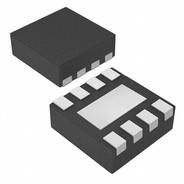
Package
The TPS61252DSGT comes in a small, surface-mount package known as VQFN (Very Thin Quad Flat No-Lead). This package offers excellent thermal performance and ease of integration into compact designs.
Essence
The essence of the TPS61252DSGT lies in its ability to efficiently boost and regulate input voltages to desired output levels, making it suitable for various applications where voltage conversion is required.
Packaging/Quantity
The TPS61252DSGT is typically available in reels containing 2500 units per reel.
Specifications
- Input Voltage Range: 0.3V to 5.5V
- Output Voltage Range: 1.8V to 5.5V
- Maximum Output Current: 1A
- Quiescent Current: 17µA
- Switching Frequency: 2.4MHz
- Efficiency: Up to 95%
- Shutdown Current: <1µA
- Operating Temperature Range: -40°C to +85°C
- Package Type: VQFN
Detailed Pin Configuration
The TPS61252DSGT has the following pin configuration:
- VIN: Input voltage pin.
- EN: Enable pin for turning the device on/off.
- PG: Power good indicator pin.
- FB: Feedback pin for setting the output voltage.
- SW: Switching node pin.
- GND: Ground pin.
Functional Features
- Wide input voltage range allows compatibility with various power sources.
- High efficiency ensures minimal power loss during voltage conversion.
- Adjustable output voltage enables flexibility in different applications.
- Power good indicator provides a signal to indicate stable output voltage.
- Enable pin allows easy control of device operation.
- Low quiescent current minimizes power consumption during standby or idle periods.
- Overcurrent and thermal protection features enhance reliability and safety.
Advantages and Disadvantages
Advantages
- Wide input voltage range enables compatibility with diverse power sources.
- High efficiency reduces power dissipation and extends battery life.
- Compact package facilitates integration into space-constrained designs.
- Power good indicator enhances system monitoring and fault detection.
- Adjustable output voltage offers versatility in different applications.
Disadvantages
- Maximum output current limited to 1A, which may not be sufficient for high-power applications.
- Higher switching frequency may introduce additional noise in sensitive circuits.
Working Principles
The TPS61252DSGT operates as a step-up (boost) voltage regulator. It utilizes a high-frequency switching technique to efficiently convert lower input voltages to higher output voltages. The internal control circuitry adjusts the duty cycle of the switching transistor to regulate the output voltage within the desired range. This switching action minimizes power loss and maximizes efficiency.
Detailed Application Field Plans
The TPS61252DSGT finds applications in various fields, including:
Portable Electronics: It can be used to boost battery voltage to power display modules, microcontrollers, and other components in smartphones, tablets, and portable media players.
IoT Devices: The TPS61252DSGT is suitable for powering low-power IoT devices that operate on low input voltages, such as wireless sensors, smart home devices, and wearable gadgets.
Automotive Electronics: It can be employed in automotive applications to regulate voltage levels for powering infotainment systems, navigation units, and other electronic modules.
Industrial Automation: The TPS61252DSGT can be utilized in industrial automation systems to convert lower voltage signals to higher levels required by various control circuits and sensors.
Detailed and Complete Alternative Models
- TPS61250DSGT: Similar to the TPS61252DSGT, but with a lower maximum output current of 500mA.
- TPS61253DSGT: Similar to the TPS61252DSGT, but with a higher maximum output current of 1.5A.
- TPS61254DSGT: Similar to the TPS61252DSGT, but with a higher maximum output current of 2A.
These alternative models offer different output current capabilities while maintaining similar functionality and characteristics to the TPS61252DSGT.
In conclusion, the TPS61252DSGT is a versatile voltage regulator that efficiently boosts and regulates input volt
قم بإدراج 10 أسئلة وإجابات شائعة تتعلق بتطبيق TPS61252DSGT في الحلول التقنية
Sure! Here are 10 common questions and answers related to the application of TPS61252DSGT in technical solutions:
Q: What is TPS61252DSGT? A: TPS61252DSGT is a step-up (boost) DC-DC converter integrated circuit (IC) that provides efficient power conversion from a lower voltage source to a higher voltage output.
Q: What is the input voltage range of TPS61252DSGT? A: The input voltage range of TPS61252DSGT is typically between 0.3V and 5.5V.
Q: What is the output voltage range of TPS61252DSGT? A: The output voltage range of TPS61252DSGT can be adjusted from 1.8V to 5.5V using external resistors.
Q: What is the maximum output current of TPS61252DSGT? A: The maximum output current of TPS61252DSGT is typically 1.2A, but it can vary depending on the specific application and operating conditions.
Q: Can TPS61252DSGT operate with low input voltages? A: Yes, TPS61252DSGT is designed to operate efficiently even with very low input voltages, making it suitable for applications powered by single-cell batteries or energy harvesting sources.
Q: Does TPS61252DSGT have built-in protection features? A: Yes, TPS61252DSGT includes various protection features such as overcurrent protection, thermal shutdown, and undervoltage lockout to ensure safe operation.
Q: Can TPS61252DSGT be used in portable devices? A: Yes, TPS61252DSGT is commonly used in portable devices like smartphones, tablets, wearables, and IoT devices to efficiently boost the battery voltage for different components.
Q: What is the efficiency of TPS61252DSGT? A: The efficiency of TPS61252DSGT can reach up to 95% depending on the input/output voltage conditions and load current.
Q: Can TPS61252DSGT be used in automotive applications? A: Yes, TPS61252DSGT is suitable for automotive applications that require efficient voltage boosting, such as powering sensors, displays, or communication modules.
Q: Are there any evaluation boards available for TPS61252DSGT? A: Yes, Texas Instruments provides evaluation boards for TPS61252DSGT, which can help engineers quickly prototype and test their designs.
Please note that these answers are general and may vary depending on the specific application and requirements. It's always recommended to refer to the datasheet and consult with the manufacturer for detailed information.