

TC74VHC299FTEL
Product Overview
- Category: Integrated Circuit (IC)
- Use: Shift Register
- Characteristics: High-speed operation, low power consumption
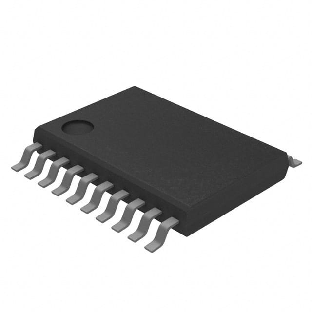
- Package: TSSOP (Thin Shrink Small Outline Package)
- Essence: 8-bit universal shift register with parallel input/output capability
- Packaging/Quantity: Tape and Reel, 2500 units per reel
Specifications
- Supply Voltage Range: 2.0V to 5.5V
- Operating Temperature Range: -40°C to +85°C
- Input/Output Compatibility: TTL, CMOS
- Maximum Clock Frequency: 200MHz
- Number of Bits: 8
- Output Drive Capability: ±6mA
- Propagation Delay Time: 4.3ns (typical)
Detailed Pin Configuration
The TC74VHC299FTEL has a total of 20 pins. The pin configuration is as follows:
- Q0 (Output)
- Q1 (Output)
- Q2 (Output)
- Q3 (Output)
- Q4 (Output)
- Q5 (Output)
- Q6 (Output)
- Q7 (Output)
- GND (Ground)
- SER (Serial Data Input)
- RCLK (Register Clock Input)
- SRCLK (Shift Register Clock Input)
- OE (Output Enable Input)
- MR (Master Reset Input)
- QA (Parallel Data Input)
- QB (Parallel Data Input)
- QC (Parallel Data Input)
- QD (Parallel Data Input)
- VCC (Power Supply)
- QH (Output)
Functional Features
- Parallel-to-Serial Conversion: Allows data to be loaded in parallel and shifted out serially.
- Serial-to-Parallel Conversion: Enables serial data to be loaded and stored in parallel.
- Universal Shift Register: Supports both serial and parallel data transfer modes.
- Output Enable Control: Allows the outputs to be enabled or disabled.
- Master Reset Function: Resets the shift register to its initial state.
Advantages and Disadvantages
Advantages: - High-speed operation enables efficient data transfer. - Low power consumption makes it suitable for battery-powered devices. - Versatile functionality with support for both serial and parallel data transfer modes.
Disadvantages: - Limited output drive capability may not be suitable for high-current applications. - Propagation delay time may affect timing-sensitive applications.
Working Principles
The TC74VHC299FTEL is an 8-bit universal shift register that can operate in both serial and parallel modes. It consists of a shift register, latch, and control logic. In the parallel mode, data is loaded into the shift register through the parallel inputs (QA to QD) and then latched into the output registers on the rising edge of the register clock (RCLK). In the serial mode, data is shifted in through the serial input (SER) and shifted out through the QH output. The output enable (OE) pin allows the outputs to be enabled or disabled, while the master reset (MR) pin resets the shift register to its initial state.
Detailed Application Field Plans
The TC74VHC299FTEL is commonly used in various applications, including:
- Data Communication Systems: Used for serial-to-parallel and parallel-to-serial conversion in communication protocols.
- Industrial Automation: Enables efficient data transfer and storage in control systems.
- Consumer Electronics: Utilized in devices such as gaming consoles, set-top boxes, and digital cameras for data manipulation.
- Automotive Electronics: Integrated into automotive control units for data processing and transmission.
- Medical Equipment: Facilitates data handling in medical devices like patient monitors and diagnostic equipment.
Detailed and Complete Alternative Models
- SN74HC299: Similar 8-bit universal shift register with parallel input/output capability, offered by Texas Instruments.
- CD74HCT299E: High-speed CMOS logic IC with an 8-bit universal shift register, manufactured by Texas Instruments.
- 74HC595: 8-bit serial-in, serial or parallel-out shift register with output latches, available from various manufacturers.
(Note: The above alternative models are provided for reference and may have different specifications and pin configurations. It is recommended to consult the respective datasheets for detailed information.)
Word count: 533 words
قم بإدراج 10 أسئلة وإجابات شائعة تتعلق بتطبيق TC74VHC299FTEL في الحلول التقنية
Sure! Here are 10 common questions and answers related to the application of TC74VHC299FTEL:
Q: What is TC74VHC299FTEL? A: TC74VHC299FTEL is a 8-bit universal shift register with parallel outputs, commonly used in digital circuits.
Q: What is the operating voltage range for TC74VHC299FTEL? A: The operating voltage range for TC74VHC299FTEL is typically between 2.0V and 5.5V.
Q: Can TC74VHC299FTEL be used in both serial and parallel data transfer modes? A: Yes, TC74VHC299FTEL can be used in both serial and parallel data transfer modes, making it versatile for various applications.
Q: What is the maximum clock frequency supported by TC74VHC299FTEL? A: The maximum clock frequency supported by TC74VHC299FTEL is typically around 100MHz.
Q: How many input/output pins does TC74VHC299FTEL have? A: TC74VHC299FTEL has a total of 20 pins, including 8 input pins and 8 output pins.
Q: Can TC74VHC299FTEL be cascaded to increase the number of bits? A: Yes, TC74VHC299FTEL can be cascaded to increase the number of bits by connecting the serial output of one shift register to the serial input of another.
Q: Does TC74VHC299FTEL support asynchronous clear functionality? A: Yes, TC74VHC299FTEL supports asynchronous clear functionality, allowing you to reset the shift register to a known state.
Q: What is the typical power consumption of TC74VHC299FTEL? A: The typical power consumption of TC74VHC299FTEL is relatively low, making it suitable for battery-powered applications.
Q: Can TC74VHC299FTEL be used in both CMOS and TTL logic systems? A: Yes, TC74VHC299FTEL is compatible with both CMOS and TTL logic systems, providing flexibility in design.
Q: Are there any specific application notes or reference designs available for TC74VHC299FTEL? A: Yes, the manufacturer provides application notes and reference designs that can help you understand and implement TC74VHC299FTEL in your technical solutions.
Please note that the answers provided here are general and may vary depending on the specific datasheet and manufacturer's documentation for TC74VHC299FTEL.