

TC74VHC540FTELM
Product Overview
- Category: Integrated Circuit (IC)
- Use: Buffer/Line Driver
- Characteristics: High-speed, low-power, voltage level shifting
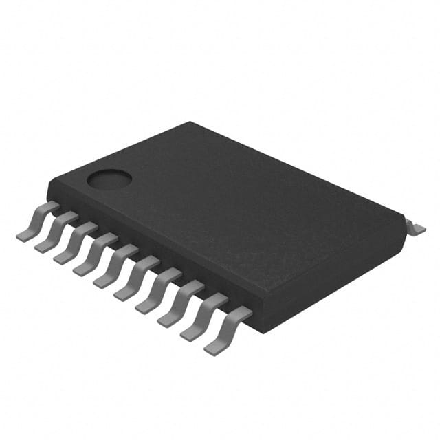
- Package: TSSOP (Thin Shrink Small Outline Package)
- Essence: Logic IC for signal buffering and voltage level conversion
- Packaging/Quantity: Tape and Reel, 2500 units per reel
Specifications
- Supply Voltage Range: 2.0V to 5.5V
- Input Voltage Range: 0V to VCC
- Output Voltage Range: 0V to VCC
- Maximum Operating Frequency: 200MHz
- Number of Channels: 8
- Input/Output Type: Non-Inverting
- Output Drive Capability: ±24mA
- Propagation Delay Time: 3.7ns (typical)
Detailed Pin Configuration
The TC74VHC540FTELM has a total of 20 pins, which are arranged as follows:
- GND - Ground
- A1 - Input/Output 1
- B1 - Input/Output 2
- Y1 - Output 1
- OE - Output Enable
- GND - Ground
- Y2 - Output 2
- B2 - Input/Output 3
- A2 - Input/Output 4
- GND - Ground
- A3 - Input/Output 5
- B3 - Input/Output 6
- Y3 - Output 3
- GND - Ground
- Y4 - Output 4
- B4 - Input/Output 7
- A4 - Input/Output 8
- VCC - Power Supply
- GND - Ground
- GND - Ground
Functional Features
- High-speed operation: The TC74VHC540FTELM is designed to operate at high frequencies, making it suitable for applications requiring fast signal buffering.
- Low-power consumption: This IC is optimized for low power consumption, making it ideal for battery-powered devices or energy-efficient systems.
- Voltage level shifting: It can convert logic signals between different voltage levels, allowing compatibility between devices operating at different voltage levels.
- Output enable control: The OE pin allows the user to enable or disable the outputs, providing flexibility in controlling the signal flow.
Advantages and Disadvantages
Advantages: - High-speed operation enables efficient signal buffering. - Low-power consumption prolongs battery life in portable devices. - Voltage level shifting capability enhances compatibility between different devices.
Disadvantages: - Limited output drive capability may not be suitable for driving heavy loads. - Propagation delay time may introduce timing issues in certain applications.
Working Principles
The TC74VHC540FTELM operates based on CMOS (Complementary Metal-Oxide-Semiconductor) technology. It utilizes a combination of NMOS (N-channel Metal-Oxide-Semiconductor) and PMOS (P-channel Metal-Oxide-Semiconductor) transistors to achieve high-speed and low-power performance. The input signals are buffered and level-shifted to match the desired output voltage levels. The output enable control allows the user to selectively enable or disable the outputs.
Detailed Application Field Plans
The TC74VHC540FTELM finds applications in various fields, including:
- Microcontrollers and Digital Systems: It can be used to interface microcontrollers with different voltage level peripherals, ensuring proper signal compatibility.
- Communication Systems: It facilitates voltage level conversion between different communication protocols, enabling seamless data transfer.
- Industrial Automation: The IC can be employed in industrial automation systems to buffer and convert signals between different control modules.
- Automotive Electronics: It is suitable for voltage level shifting in automotive electronics, such as sensor interfaces or communication buses.
Detailed and Complete Alternative Models
- SN74LV1T34DBVR: Single Buffer/Driver with similar characteristics and package (SOT-23).
- MC74VHC1GT125DF1G: Single Buffer/Driver with comparable specifications and package (SOT-353).
- 74LVC244APW: Octal Buffer/Line Driver with higher output drive capability and different package (TSSOP).
(Note: The above alternative models are provided for reference and may have slight variations in specifications and features.)
This entry provides a comprehensive overview of the TC74VHC540FTELM, including its product details, pin configuration, functional features, advantages, disadvantages, working principles, application field plans, and alternative models. With its high-speed operation, low-power consumption, and voltage level shifting capabilities, this IC offers a versatile solution for signal buffering and voltage level conversion in various electronic systems.
قم بإدراج 10 أسئلة وإجابات شائعة تتعلق بتطبيق TC74VHC540FTELM في الحلول التقنية
Sure! Here are 10 common questions and answers related to the application of TC74VHC540FTELM:
1. What is TC74VHC540FTELM? - TC74VHC540FTELM is a specific model of a voltage level translator integrated circuit (IC) that can be used in various technical solutions.
2. What is the purpose of TC74VHC540FTELM? - The purpose of TC74VHC540FTELM is to translate voltage levels between different logic families, allowing communication between devices with different voltage requirements.
3. What voltage levels can TC74VHC540FTELM translate? - TC74VHC540FTELM can translate voltage levels between 2.0V and 5.5V.
4. How many channels does TC74VHC540FTELM have? - TC74VHC540FTELM has 8 bidirectional channels, which means it can translate signals in both directions.
5. What is the maximum data rate supported by TC74VHC540FTELM? - TC74VHC540FTELM supports a maximum data rate of 200 Mbps.
6. Can TC74VHC540FTELM be used in both digital and analog applications? - No, TC74VHC540FTELM is specifically designed for digital applications and should not be used for analog signals.
7. Is TC74VHC540FTELM compatible with CMOS and TTL logic families? - Yes, TC74VHC540FTELM is compatible with both CMOS and TTL logic families.
8. Does TC74VHC540FTELM require external power supply decoupling capacitors? - Yes, it is recommended to use external power supply decoupling capacitors for stable operation of TC74VHC540FTELM.
9. Can TC74VHC540FTELM be used in high-speed applications? - Yes, TC74VHC540FTELM is suitable for high-speed applications due to its fast propagation delay and transition times.
10. What package does TC74VHC540FTELM come in? - TC74VHC540FTELM is available in a TSSOP (Thin Shrink Small Outline Package) package with 20 pins.
Please note that these answers are general and may vary depending on the specific application and requirements. It is always recommended to refer to the datasheet and consult the manufacturer for detailed information.