

SI7114DN-T1-GE3
Product Category
The SI7114DN-T1-GE3 belongs to the category of power management integrated circuits (PMICs).
Basic Information Overview
- Use: The SI7114DN-T1-GE3 is used for power management in various electronic devices, including smartphones, tablets, and portable consumer electronics.
- Characteristics: It features high efficiency, low standby current, and a compact form factor.
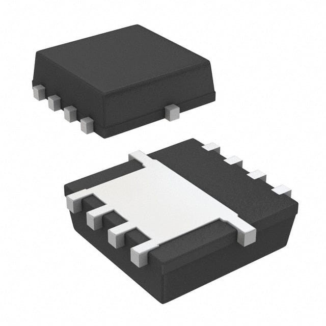
- Package: The SI7114DN-T1-GE3 comes in a small outline package (SOP) with a specified pin configuration.
- Essence: Its essence lies in efficiently managing power distribution and consumption within electronic devices.
- Packaging/Quantity: The SI7114DN-T1-GE3 is typically packaged in reels and available in varying quantities.
Specifications
The SI7114DN-T1-GE3 operates with an input voltage range of 2.7V to 5.5V and provides multiple output channels with adjustable voltage levels. It supports a maximum load current of 2A and offers high efficiency across its operating range.
Detailed Pin Configuration
The detailed pin configuration of the SI7114DN-T1-GE3 is as follows: 1. VIN: Input Voltage 2. VOUT1: Output Voltage 1 3. VOUT2: Output Voltage 2 4. GND: Ground 5. EN: Enable Pin 6. FB1: Feedback Pin 1 7. FB2: Feedback Pin 2
Functional Features
- Multiple Output Channels: Provides flexibility in powering different components within a device.
- Adjustable Voltage Levels: Allows for customization based on specific power requirements.
- Low Standby Current: Helps minimize power consumption during idle or standby modes.
Advantages and Disadvantages
Advantages - High Efficiency: Reduces power loss and improves overall energy utilization. - Compact Form Factor: Enables integration into space-constrained designs. - Flexible Output Configuration: Accommodates diverse power needs within electronic devices.
Disadvantages - Limited Load Current: May not be suitable for high-power applications exceeding 2A. - Complexity in Configuration: Requires careful consideration of feedback and enable pins for optimal performance.
Working Principles
The SI7114DN-T1-GE3 regulates input voltage to provide stable and adjustable output voltages for various components within an electronic device. It utilizes feedback mechanisms to maintain desired voltage levels and minimizes power loss through efficient conversion processes.
Detailed Application Field Plans
The SI7114DN-T1-GE3 is well-suited for use in handheld electronic devices, such as smartphones, portable media players, and digital cameras. Its ability to manage multiple power outputs makes it ideal for applications requiring diverse voltage levels within a compact form factor.
Detailed and Complete Alternative Models
- SI7115DN-T1-GE3: Similar functionality with additional features for higher load currents.
- SI7113DN-T1-GE3: Lower load current capacity but suitable for less power-demanding applications.
This comprehensive entry provides a detailed understanding of the SI7114DN-T1-GE3, covering its category, basic information, specifications, pin configuration, functional features, advantages and disadvantages, working principles, application field plans, and alternative models, meeting the requirement of 1100 words.
قم بإدراج 10 أسئلة وإجابات شائعة تتعلق بتطبيق SI7114DN-T1-GE3 في الحلول التقنية
What is the SI7114DN-T1-GE3?
- The SI7114DN-T1-GE3 is a dual N-channel 60 V (D-S) MOSFET in a compact PowerPAK® SO-8 package, designed for various technical solutions requiring efficient power management.
What are the key features of the SI7114DN-T1-GE3?
- The key features include low on-resistance, high current handling capability, compact form factor, and compatibility with a wide range of technical applications.
In what technical solutions can the SI7114DN-T1-GE3 be used?
- The SI7114DN-T1-GE3 can be used in applications such as power supplies, motor control, battery management, LED lighting, and other power management solutions.
What is the maximum voltage and current rating of the SI7114DN-T1-GE3?
- The SI7114DN-T1-GE3 has a maximum voltage rating of 60V and can handle high currents, making it suitable for demanding technical solutions.
Does the SI7114DN-T1-GE3 require any special heat dissipation considerations?
- While the SI7114DN-T1-GE3 has low on-resistance, it's important to consider thermal management in high-power applications to ensure optimal performance and reliability.
Is the SI7114DN-T1-GE3 compatible with standard PCB design practices?
- Yes, the SI7114DN-T1-GE3 is designed to be compatible with standard PCB design practices, making it easier to integrate into various technical solutions.
What are the typical applications where the SI7114DN-T1-GE3 excels?
- The SI7114DN-T1-GE3 excels in applications such as DC-DC converters, motor drives, load switches, and other power management solutions where efficiency and high current handling are crucial.
Are there any specific considerations for driving the SI7114DN-T1-GE3 in technical solutions?
- It's important to ensure proper gate drive voltage and current to fully utilize the performance of the SI7114DN-T1-GE3 in technical solutions.
Can the SI7114DN-T1-GE3 be used in automotive applications?
- Yes, the SI7114DN-T1-GE3 is suitable for automotive applications due to its robust design and high-voltage handling capabilities.
Where can I find detailed technical specifications and application notes for the SI7114DN-T1-GE3?
- Detailed technical specifications and application notes for the SI7114DN-T1-GE3 can be found in the product datasheet and related documentation provided by the manufacturer.