

XC2C512-7FG324C
Product Overview
Category
XC2C512-7FG324C belongs to the category of programmable logic devices (PLDs).
Use
This product is used for digital circuit design and implementation in various electronic applications.
Characteristics
- Programmable: The XC2C512-7FG324C can be programmed to perform specific functions as per the user's requirements.
- High-density: It offers a large number of configurable logic blocks, allowing complex designs to be implemented.
- Versatile: The device supports a wide range of applications due to its flexible architecture.
- Low power consumption: The XC2C512-7FG324C is designed to operate efficiently with minimal power consumption.
Package
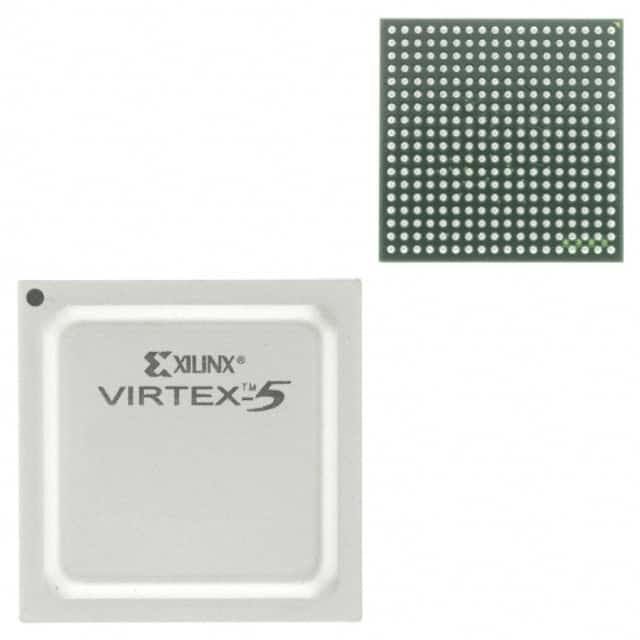
The XC2C512-7FG324C is available in a FG324 package.
Essence
The essence of XC2C512-7FG324C lies in its ability to provide a reconfigurable hardware platform for implementing digital circuits.
Packaging/Quantity
This product is typically packaged individually and is available in varying quantities depending on the supplier.
Specifications
- Device type: Programmable Logic Device (PLD)
- Family: XC2C
- Density: 512 macrocells
- Speed grade: -7
- Package: FG324
- Operating voltage: 3.3V
- I/O standards: LVTTL, LVCMOS
Detailed Pin Configuration
The XC2C512-7FG324C has a total of 324 pins. The pin configuration is as follows:
- Pin 1: VCCIO
- Pin 2: GND
- Pin 3: IO_0
- Pin 4: IO_1
- ...
- Pin 323: IO_322
- Pin 324: IO_323
Functional Features
- High-speed performance: The XC2C512-7FG324C offers fast operation, enabling efficient execution of complex digital designs.
- Reconfigurability: The device can be reprogrammed multiple times, allowing for design modifications and updates.
- Flexible I/O options: It supports various input/output standards, making it compatible with different interface requirements.
- On-chip memory: The XC2C512-7FG324C includes embedded memory blocks for storing configuration data and user-defined logic.
Advantages and Disadvantages
Advantages
- Versatile and flexible design capabilities
- High-density implementation for complex circuits
- Low power consumption
- Cost-effective solution compared to custom ASICs
Disadvantages
- Limited resources compared to larger PLDs or FPGAs
- Longer development time due to programming and verification processes
- Higher cost compared to simpler programmable devices like CPLDs
Working Principles
The XC2C512-7FG324C operates based on the principles of field-programmable gate arrays (FPGAs). It consists of configurable logic blocks (CLBs), interconnect resources, and input/output blocks. The CLBs can be programmed to implement desired logic functions, while the interconnect resources facilitate communication between different blocks. The input/output blocks provide connectivity to external devices.
Detailed Application Field Plans
The XC2C512-7FG324C finds applications in various fields, including:
- Communications: Used in network routers, switches, and wireless communication systems.
- Industrial automation: Employed in control systems, robotics, and process automation.
- Automotive electronics: Utilized in engine control units, infotainment systems, and driver assistance systems.
- Consumer electronics: Integrated into smart TVs, gaming consoles, and home automation devices.
- Medical devices: Applied in medical imaging equipment, patient monitoring systems, and laboratory instruments.
Detailed and Complete Alternative Models
- XC2C256-7FG324C: A lower-density version of the XC2C512-7FG324C with 256 macrocells.
- XC2C384-7FG324C: A higher-density variant with 384 macrocells.
- XC2C768-7FG324C: An even higher-density model with 768 macrocells.
These alternative models provide options for different design requirements, allowing users to choose the most suitable PLD based on their project needs.
Word count: 550 words
قم بإدراج 10 أسئلة وإجابات شائعة تتعلق بتطبيق XC2C512-7FG324C في الحلول التقنية
Sure! Here are 10 common questions and answers related to the application of XC2C512-7FG324C in technical solutions:
Q: What is XC2C512-7FG324C? A: XC2C512-7FG324C is a specific model of Field Programmable Gate Array (FPGA) manufactured by Xilinx.
Q: What are the key features of XC2C512-7FG324C? A: Some key features of XC2C512-7FG324C include 512 macrocells, 7ns maximum delay, and a 324-pin Fine-Pitch Ball Grid Array (FBGA) package.
Q: How can XC2C512-7FG324C be used in technical solutions? A: XC2C512-7FG324C can be used to implement digital logic circuits, perform complex computations, and interface with other electronic components.
Q: What programming languages can be used to program XC2C512-7FG324C? A: XC2C512-7FG324C can be programmed using Hardware Description Languages (HDLs) such as VHDL or Verilog.
Q: Can XC2C512-7FG324C be reprogrammed after it has been initially programmed? A: Yes, XC2C512-7FG324C is a reprogrammable FPGA, which means its configuration can be modified multiple times.
Q: What tools are required to program XC2C512-7FG324C? A: To program XC2C512-7FG324C, you will need a compatible development board, a programming cable, and Xilinx's Integrated Development Environment (IDE) software.
Q: What are some typical applications of XC2C512-7FG324C? A: XC2C512-7FG324C can be used in various applications such as digital signal processing, robotics, aerospace systems, and telecommunications.
Q: What is the power supply requirement for XC2C512-7FG324C? A: XC2C512-7FG324C typically operates at a voltage range of 1.14V to 1.26V, with a maximum power consumption of around 1.5W.
Q: Can XC2C512-7FG324C interface with other electronic components? A: Yes, XC2C512-7FG324C can interface with other components through its I/O pins, which can be configured as inputs or outputs.
Q: Are there any limitations or considerations when using XC2C512-7FG324C? A: Some considerations include the need for proper cooling due to power dissipation, understanding the limitations of the available macrocells, and ensuring compatibility with other system components.
Please note that these answers are general and may vary depending on specific use cases and requirements.