

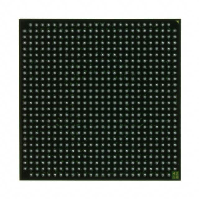
XC2VP4-5FFG672C
Product Overview
Category
XC2VP4-5FFG672C belongs to the category of Field Programmable Gate Arrays (FPGAs).
Use
This FPGA is primarily used for digital logic implementation and prototyping in various electronic systems.
Characteristics
- High-performance programmable logic device
- Offers flexibility and reconfigurability
- Provides fast time-to-market for electronic designs
- Supports complex digital circuitry
Package
XC2VP4-5FFG672C comes in a 672-pin Fine-Pitch Ball Grid Array (FBGA) package.
Essence
The essence of XC2VP4-5FFG672C lies in its ability to provide a customizable and versatile platform for implementing digital circuits.
Packaging/Quantity
Each package of XC2VP4-5FFG672C contains one unit of the FPGA.
Specifications
- Logic Cells: 4,608
- Flip-Flops: 9,216
- Block RAM: 1.3 Mb
- DSP Slices: 32
- Maximum Frequency: 500 MHz
- I/O Pins: 400
- Operating Voltage: 1.2V
Detailed Pin Configuration
The detailed pin configuration of XC2VP4-5FFG672C can be found in the manufacturer's datasheet.
Functional Features
XC2VP4-5FFG672C offers the following functional features:
- Configurable logic blocks for implementing custom digital circuits
- Dedicated DSP slices for efficient signal processing
- Integrated memory blocks for data storage
- Flexible I/O pins for interfacing with external devices
- Clock management resources for precise timing control
Advantages and Disadvantages
Advantages
- High level of customization and reconfigurability
- Fast development cycle due to programmable nature
- Suitable for prototyping and low-volume production
- Supports complex digital designs
Disadvantages
- Higher cost compared to fixed-function integrated circuits
- Limited performance compared to application-specific hardware
- Requires expertise in FPGA programming and design
Working Principles
XC2VP4-5FFG672C operates based on the principles of reconfigurable logic. It consists of configurable logic blocks, memory elements, and interconnect resources. The device can be programmed to implement various digital circuits by configuring the interconnections between logic elements.
Detailed Application Field Plans
XC2VP4-5FFG672C finds applications in a wide range of fields, including:
- Telecommunications: Used in base stations, network routers, and communication equipment.
- Aerospace and Defense: Employed in radar systems, avionics, and military communication devices.
- Industrial Automation: Utilized in control systems, robotics, and factory automation.
- Medical Electronics: Applied in medical imaging, patient monitoring, and diagnostic equipment.
- Automotive: Used in advanced driver assistance systems (ADAS), infotainment systems, and engine control units.
Detailed and Complete Alternative Models
Some alternative models to XC2VP4-5FFG672C are:
- XC2VP7-6FFG672C: Offers higher logic capacity and performance.
- XC2VP30-7FFG672C: Provides increased DSP slices for signal processing applications.
- XC2VP50-5FFG672C: Offers larger block RAM capacity for data storage requirements.
These alternative models cater to different design needs and can be chosen based on specific project requirements.
Word count: 410
قم بإدراج 10 أسئلة وإجابات شائعة تتعلق بتطبيق XC2VP4-5FFG672C في الحلول التقنية
Sure! Here are 10 common questions and answers related to the application of XC2VP4-5FFG672C in technical solutions:
Question: What is XC2VP4-5FFG672C?
Answer: XC2VP4-5FFG672C is a specific model of Field Programmable Gate Array (FPGA) manufactured by Xilinx.Question: What are the key features of XC2VP4-5FFG672C?
Answer: Some key features of XC2VP4-5FFG672C include 4 million system gates, 672-pin Fine-Pitch Ball Grid Array (FBGA) package, and support for various I/O standards.Question: In what applications can XC2VP4-5FFG672C be used?
Answer: XC2VP4-5FFG672C can be used in a wide range of applications such as telecommunications, networking, industrial automation, and high-performance computing.Question: What is the maximum operating frequency of XC2VP4-5FFG672C?
Answer: The maximum operating frequency of XC2VP4-5FFG672C depends on the design and implementation, but it can typically reach several hundred megahertz.Question: Can XC2VP4-5FFG672C be reprogrammed after deployment?
Answer: Yes, XC2VP4-5FFG672C is a field-programmable device, which means it can be reprogrammed even after it has been deployed in a system.Question: What development tools are available for programming XC2VP4-5FFG672C?
Answer: Xilinx provides a suite of development tools, including Vivado Design Suite, that can be used to program and configure XC2VP4-5FFG672C.Question: What is the power consumption of XC2VP4-5FFG672C?
Answer: The power consumption of XC2VP4-5FFG672C depends on the specific design and operating conditions, but it typically ranges from a few watts to tens of watts.Question: Can XC2VP4-5FFG672C interface with other components or devices?
Answer: Yes, XC2VP4-5FFG672C supports various I/O standards and can interface with other components or devices such as memory, sensors, and communication interfaces.Question: Are there any limitations or considerations when using XC2VP4-5FFG672C?
Answer: Some considerations include the need for proper power management, thermal dissipation, and ensuring compatibility with other system components.Question: Where can I find more information about XC2VP4-5FFG672C?
Answer: You can find more detailed information about XC2VP4-5FFG672C in the datasheet provided by Xilinx or by visiting their official website.