

XC3S400A-4FGG320C
Product Overview
Category
The XC3S400A-4FGG320C belongs to the category of Field-Programmable Gate Arrays (FPGAs).
Use
FPGAs are integrated circuits that can be programmed and reprogrammed to perform various digital functions. The XC3S400A-4FGG320C is specifically designed for high-performance applications.
Characteristics
- High-speed performance: The XC3S400A-4FGG320C offers fast processing capabilities, making it suitable for demanding applications.
- Programmability: As an FPGA, this product allows users to configure its internal logic according to their specific requirements.
- Versatility: The XC3S400A-4FGG320C can be used in a wide range of applications due to its flexible nature.
Package
The XC3S400A-4FGG320C comes in a compact and durable package, ensuring easy handling and protection against external factors.
Essence
The essence of the XC3S400A-4FGG320C lies in its ability to provide customizable digital functionality through programmable logic.
Packaging/Quantity
This product is typically packaged individually and is available in varying quantities depending on the supplier.
Specifications
- Model: XC3S400A-4FGG320C
- Logic Cells: 400,000
- Operating Voltage: 1.2V
- Maximum Frequency: 500 MHz
- I/O Pins: 320
- Package Type: Fine-Pitch Ball Grid Array (FBGA)
- Temperature Range: -40°C to +100°C
Detailed Pin Configuration
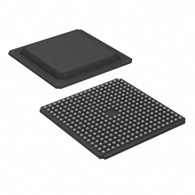
The XC3S400A-4FGG320C has a total of 320 I/O pins, which are arranged in a specific configuration. The pinout diagram and detailed pin descriptions can be found in the product datasheet.
Functional Features
- High-speed data processing: The XC3S400A-4FGG320C offers fast data processing capabilities, making it suitable for applications that require real-time performance.
- Flexible logic configuration: With its programmable nature, this FPGA allows users to implement complex digital functions by configuring its internal logic cells.
- On-chip memory: The XC3S400A-4FGG320C includes embedded memory blocks, enabling efficient storage and retrieval of data during operation.
- Multiple I/O standards: This product supports various input/output voltage standards, allowing seamless integration with different external devices.
Advantages and Disadvantages
Advantages
- Customizability: The XC3S400A-4FGG320C provides users with the flexibility to design and implement their own digital circuits.
- High-performance capabilities: This FPGA offers fast processing speeds, making it suitable for demanding applications.
- Cost-effective solution: FPGAs eliminate the need for custom-designed ASICs, reducing development costs for certain applications.
Disadvantages
- Complexity: Programming and configuring an FPGA requires specialized knowledge and expertise.
- Power consumption: FPGAs tend to consume more power compared to dedicated application-specific integrated circuits (ASICs).
- Limited scalability: While FPGAs offer flexibility, they may not be the most scalable solution for certain applications that require large-scale production.
Working Principles
The XC3S400A-4FGG320C operates based on the principles of reconfigurable logic. It consists of a matrix of configurable logic blocks interconnected through programmable routing resources. Users can program the FPGA using hardware description languages (HDL) or graphical tools to define the desired functionality. Once programmed, the FPGA executes the configured logic operations.
Detailed Application Field Plans
The XC3S400A-4FGG320C finds applications in various fields, including:
- Communications: This FPGA can be used in high-speed data communication systems, such as network routers and switches, to handle complex packet processing tasks.
- Industrial Automation: The XC3S400A-4FGG320C is suitable for industrial control systems, enabling real-time monitoring and control of manufacturing processes.
- Aerospace and Defense: FPGAs are widely used in aerospace and defense applications, including radar systems, avionics, and secure communications, due to their high-performance capabilities and reconfigurability.
Detailed and Complete Alternative Models
- XC3S200A-4VQG100C: A lower-capacity variant of the XC3S400A-4FGG320C, offering 200,000 logic cells and 100 I/O pins.
- XC3S1000-4FT256C: A higher-capacity FPGA with 1,000,000 logic cells and 256 I/O pins, suitable for more complex applications.
- XC6SLX9-2TQG144C: An alternative model from a different FPGA series,
قم بإدراج 10 أسئلة وإجابات شائعة تتعلق بتطبيق XC3S400A-4FGG320C في الحلول التقنية
Sure! Here are 10 common questions and answers related to the application of XC3S400A-4FGG320C in technical solutions:
Q: What is XC3S400A-4FGG320C? A: XC3S400A-4FGG320C is a field-programmable gate array (FPGA) manufactured by Xilinx. It offers 400,000 system gates and is designed for high-performance applications.
Q: What are some typical applications of XC3S400A-4FGG320C? A: XC3S400A-4FGG320C can be used in various applications such as digital signal processing, embedded systems, telecommunications, industrial automation, and aerospace.
Q: How does XC3S400A-4FGG320C differ from other FPGAs? A: XC3S400A-4FGG320C stands out with its high gate count, low power consumption, and advanced features like integrated PowerPC processors and DSP slices.
Q: Can XC3S400A-4FGG320C be programmed using VHDL or Verilog? A: Yes, XC3S400A-4FGG320C can be programmed using both VHDL and Verilog hardware description languages.
Q: What development tools are available for programming XC3S400A-4FGG320C? A: Xilinx provides Vivado Design Suite, which includes software tools for designing, simulating, synthesizing, and programming XC3S400A-4FGG320C.
Q: Is XC3S400A-4FGG320C suitable for high-speed data processing? A: Yes, XC3S400A-4FGG320C supports high-speed interfaces like DDR3 memory, PCIe, and Gigabit Ethernet, making it suitable for demanding data processing applications.
Q: Can XC3S400A-4FGG320C be used in safety-critical systems? A: Yes, XC3S400A-4FGG320C offers built-in features like error correction codes (ECC) and triple-module redundancy (TMR), making it suitable for safety-critical applications.
Q: What is the power consumption of XC3S400A-4FGG320C? A: The power consumption of XC3S400A-4FGG320C depends on the specific design and operating conditions but typically ranges from a few watts to tens of watts.
Q: Can XC3S400A-4FGG320C be reprogrammed multiple times? A: Yes, XC3S400A-4FGG320C is a reprogrammable FPGA, allowing users to modify and reconfigure the design multiple times during its lifespan.
Q: Are there any limitations or considerations when using XC3S400A-4FGG320C? A: Some considerations include power supply requirements, thermal management, I/O voltage levels, and ensuring proper timing constraints for reliable operation. It's important to consult the datasheet and reference designs provided by Xilinx for detailed guidelines.
Please note that these answers are general and may vary depending on specific design requirements and implementation details.