

XC4008E-3PC84I
Product Overview
Category
XC4008E-3PC84I belongs to the category of programmable logic devices (PLDs).
Use
This product is primarily used in digital circuit design and implementation. It provides a flexible and customizable solution for various applications.
Characteristics
- Programmable: The XC4008E-3PC84I can be programmed to perform specific functions, allowing for customization according to the requirements of the application.
- High Integration: This PLD integrates multiple logic gates, flip-flops, and other components into a single device, reducing the need for external components.
- Versatile: It supports a wide range of applications, including data processing, control systems, and communication devices.
- Low Power Consumption: The XC4008E-3PC84I is designed to operate efficiently with minimal power consumption.
- Reliable: It offers high reliability and stability, ensuring consistent performance over extended periods.
Package and Quantity
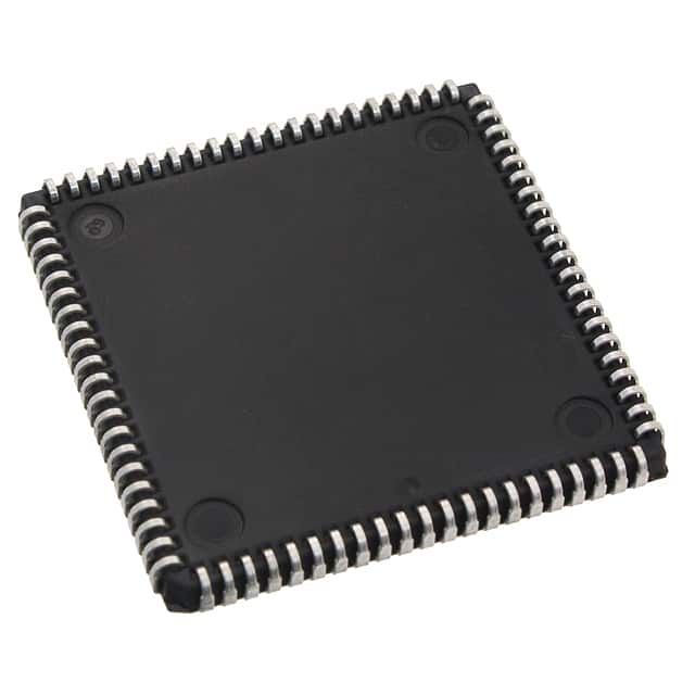
The XC4008E-3PC84I is available in a 84-pin plastic package. Each package contains one unit of the PLD.
Specifications
- Logic Cells: 4008
- Maximum Operating Frequency: 100 MHz
- Input/Output Pins: 84
- Supply Voltage: 3.3V
- Operating Temperature Range: -40°C to +85°C
- Programming Technology: In-system programmable (ISP)
Pin Configuration
The detailed pin configuration of XC4008E-3PC84I can be found in the datasheet provided by the manufacturer.
Functional Features
- Flexible Logic Implementation: The XC4008E-3PC84I allows users to implement complex logic functions using its programmable architecture.
- Fast Operation: With a maximum operating frequency of 100 MHz, this PLD enables high-speed data processing.
- I/O Flexibility: The 84 input/output pins provide versatility in connecting to external devices and circuits.
- In-system Programmability: The ISP technology allows for easy reprogramming of the device without the need for physical replacement.
Advantages
- Customizable: The XC4008E-3PC84I offers the ability to create tailored logic functions, providing a solution that precisely meets the requirements of the application.
- Cost-effective: By integrating multiple components into a single device, it reduces the need for additional hardware, resulting in cost savings.
- Time-efficient: The programmable nature of this PLD eliminates the need for redesigning and manufacturing custom circuit boards, saving time in the development process.
Disadvantages
- Complexity: Programming and configuring the XC4008E-3PC84I may require specialized knowledge and expertise.
- Limited Resources: The number of logic cells and I/O pins may be insufficient for highly complex applications.
Working Principles
The XC4008E-3PC84I operates based on the principles of digital logic. It consists of configurable logic blocks (CLBs), interconnect resources, and input/output blocks (IOBs). The CLBs can be programmed to implement various logic functions, while the interconnect resources facilitate the routing of signals between different components. The IOBs provide the interface between the PLD and external devices.
Application Field Plans
The XC4008E-3PC84I finds applications in various fields, including: 1. Industrial Automation: It can be used in control systems for machinery and equipment. 2. Telecommunications: This PLD is suitable for designing communication devices such as routers and switches. 3. Automotive Electronics: It can be utilized in automotive control systems and infotainment systems. 4. Consumer Electronics: The XC4008E-3PC84I can be employed in the design of gaming consoles, home appliances, and multimedia devices.
Alternative Models
- XC4008E-4PC84I: Similar to XC4008E-3PC84I, but with additional logic cells for more complex applications.
- XC4008EX-3PC84I: A higher-performance version of XC4008E-3PC84I with increased operating frequency.
Note: For a comprehensive list of alternative models, please refer to the manufacturer's documentation.
Word count: 529 words
قم بإدراج 10 أسئلة وإجابات شائعة تتعلق بتطبيق XC4008E-3PC84I في الحلول التقنية
Sure! Here are 10 common questions and answers related to the application of XC4008E-3PC84I in technical solutions:
Q: What is XC4008E-3PC84I? A: XC4008E-3PC84I is a specific model of Field Programmable Gate Array (FPGA) manufactured by Xilinx.
Q: What are the key features of XC4008E-3PC84I? A: Some key features of XC4008E-3PC84I include 4000 logic cells, 8 input/output blocks, 84-pin plastic package, and a maximum operating frequency of 100 MHz.
Q: In what applications can XC4008E-3PC84I be used? A: XC4008E-3PC84I can be used in various applications such as digital signal processing, telecommunications, industrial control systems, and automotive electronics.
Q: How does XC4008E-3PC84I differ from other FPGAs? A: XC4008E-3PC84I offers a balance between performance and cost-effectiveness, making it suitable for mid-range applications. It also has a good number of logic cells and I/O blocks for its size.
Q: Can XC4008E-3PC84I be reprogrammed after deployment? A: Yes, XC4008E-3PC84I is a field-programmable device, which means it can be reprogrammed even after it has been deployed in a system.
Q: What programming languages can be used with XC4008E-3PC84I? A: XC4008E-3PC84I can be programmed using Hardware Description Languages (HDLs) such as VHDL or Verilog.
Q: What development tools are available for XC4008E-3PC84I? A: Xilinx provides a range of development tools, including Vivado Design Suite, which can be used to design, simulate, and program XC4008E-3PC84I.
Q: Can XC4008E-3PC84I interface with other components in a system? A: Yes, XC4008E-3PC84I has multiple I/O blocks that allow it to interface with other components such as sensors, memory modules, and communication interfaces.
Q: What is the power consumption of XC4008E-3PC84I? A: The power consumption of XC4008E-3PC84I depends on the specific design and operating conditions, but it typically ranges from a few hundred milliwatts to a few watts.
Q: Are there any limitations or considerations when using XC4008E-3PC84I? A: Some considerations include the limited number of logic cells and I/O blocks compared to higher-end FPGAs, as well as the need for proper thermal management due to power dissipation. Additionally, compatibility with other system components should be verified before integration.
Please note that these answers are general and may vary depending on the specific requirements and use cases.