

XC4010E-3PC84I
Product Overview
Category
The XC4010E-3PC84I belongs to the category of programmable logic devices (PLDs).
Use
This product is widely used in digital circuit design and implementation. It provides a flexible and customizable solution for various applications.
Characteristics
- Programmable: The XC4010E-3PC84I can be programmed to perform specific functions based on user requirements.
- High Integration: It offers a high level of integration, allowing multiple logic functions to be implemented within a single device.
- Versatile: This PLD supports a wide range of applications, including data processing, control systems, and communication protocols.
- Low Power Consumption: The XC4010E-3PC84I is designed to operate efficiently with low power consumption.
Package and Quantity
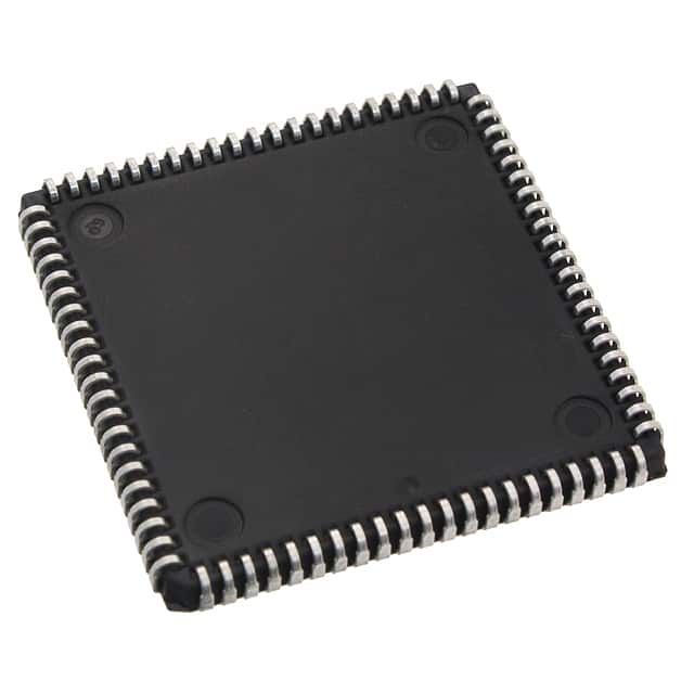
The XC4010E-3PC84I comes in a 84-pin plastic package. Each package contains one unit of the PLD.
Specifications
- Operating Voltage: 3.3V
- Maximum Operating Frequency: 50 MHz
- Number of Logic Cells: 400
- Number of I/O Pins: 68
- Maximum User I/Os: 56
- On-Chip RAM: 2,000 bits
- On-Chip ROM: 8,000 bits
- Programmable Gates: 10,000
Detailed Pin Configuration
The XC4010E-3PC84I has a total of 84 pins. Here is a detailed pin configuration:
- VCCIO
- GND
- IO0
- IO1
- IO2
- IO3
- IO4
- IO5
- IO6
- IO7
- IO8
- IO9
- IO10
- IO11
- IO12
- IO13
- IO14
- IO15
- IO16
- IO17
- IO18
- IO19
- IO20
- IO21
- IO22
- IO23
- IO24
- IO25
- IO26
- IO27
- IO28
- IO29
- IO30
- IO31
- IO32
- IO33
- IO34
- IO35
- IO36
- IO37
- IO38
- IO39
- IO40
- IO41
- IO42
- IO43
- IO44
- IO45
- IO46
- IO47
- IO48
- IO49
- IO50
- IO51
- IO52
- IO53
- IO54
- IO55
- IO56
- IO57
- IO58
- IO59
- IO60
- IO61
- IO62
- IO63
- IO64
- IO65
- IO66
- IO67
- IO68
- GND
- VCCIO
- TCK
- TMS
- TDI
- TDO
- GND
- VCCIO
- GND
- VCC
- GND
- VCC
- GND
Functional Features
The XC4010E-3PC84I offers the following functional features:
- Programmable Logic Cells: The PLD contains a large number of logic cells that can be configured to perform various functions.
- I/O Pins: It provides a sufficient number of I/O pins for interfacing with external devices.
- On-Chip Memory: The built-in RAM and ROM allow for efficient data storage and retrieval.
- Clock Management: The device supports clock signals for synchronous operation.
- Flexible Configuration: The XC4010E-3PC84I can be reprogrammed multiple times, allowing for design modifications and updates.
Advantages and Disadvantages
Advantages
- Versatility: The XC4010E-3PC84I can be used in a wide range of applications due to its programmability.
- Integration: It offers high integration, reducing the need for additional components.
- Customizability: Users can program the PLD to meet their specific requirements.
- Low Power Consumption: The device operates efficiently with low power consumption.
Disadvantages
- Complexity: Programming and configuring the XC4010E-3PC84I may require specialized knowledge and expertise.
- Limited Resources: The PLD has a finite number of logic cells and
قم بإدراج 10 أسئلة وإجابات شائعة تتعلق بتطبيق XC4010E-3PC84I في الحلول التقنية
Sure! Here are 10 common questions and answers related to the application of XC4010E-3PC84I in technical solutions:
Q: What is XC4010E-3PC84I? A: XC4010E-3PC84I is a specific model of Field Programmable Gate Array (FPGA) manufactured by Xilinx.
Q: What are the key features of XC4010E-3PC84I? A: Some key features of XC4010E-3PC84I include 4000 logic cells, 84-pin plastic package, and a maximum operating frequency of 100 MHz.
Q: How can XC4010E-3PC84I be used in technical solutions? A: XC4010E-3PC84I can be used in various applications such as digital signal processing, embedded systems, telecommunications, and industrial automation.
Q: What programming languages can be used with XC4010E-3PC84I? A: XC4010E-3PC84I can be programmed using Hardware Description Languages (HDLs) like VHDL or Verilog.
Q: Can XC4010E-3PC84I be reprogrammed after initial configuration? A: Yes, XC4010E-3PC84I is a reprogrammable FPGA, allowing for flexibility in design changes and updates.
Q: What tools are available for designing with XC4010E-3PC84I? A: Xilinx provides software tools like Vivado or ISE Design Suite that enable designers to create, simulate, and implement designs using XC4010E-3PC84I.
Q: What is the power consumption of XC4010E-3PC84I? A: The power consumption of XC4010E-3PC84I depends on the specific design and usage, but it typically operates within a low power range.
Q: Can XC4010E-3PC84I interface with other components or devices? A: Yes, XC4010E-3PC84I can interface with various peripherals and devices through its I/O pins, allowing for integration into larger systems.
Q: Are there any limitations or constraints when using XC4010E-3PC84I? A: XC4010E-3PC84I has a limited number of logic cells and I/O pins, so complex designs may require higher-capacity FPGAs.
Q: Where can I find more information about XC4010E-3PC84I and its applications? A: Xilinx's official website, technical documentation, and online forums are great resources for detailed information and application examples of XC4010E-3PC84I.